Wafer grade testing and salient point process and chip struture with testing pad

A chip structure and test pad technology, applied in semiconductor/solid-state device testing/measurement, semiconductor devices, electrical components, etc., can solve problems such as damage to the internal integrated circuit of the chip 100, affecting the normal operation of the internal integrated circuit, etc., to reduce the process Cost and process cycle, the effect of reducing process steps

Inactive Publication Date: 2003-08-13
VIA TECH INC
View PDF0 Cites 16 Cited by
  • Summary
  • Abstract
  • Description
  • Claims
  • Application Information

AI Technical Summary

Problems solved by technology

However, as a result of over-travel of the probes 12 of the probe card 10, the internal integrated circuits of the wafer 1

Method used


Image

  • Wafer grade testing and salient point process and chip struture with testing pad
  • Wafer grade testing and salient point process and chip struture with testing pad
  • Wafer grade testing and salient point process and chip struture with testing pad

Examples


Embodiment Construction

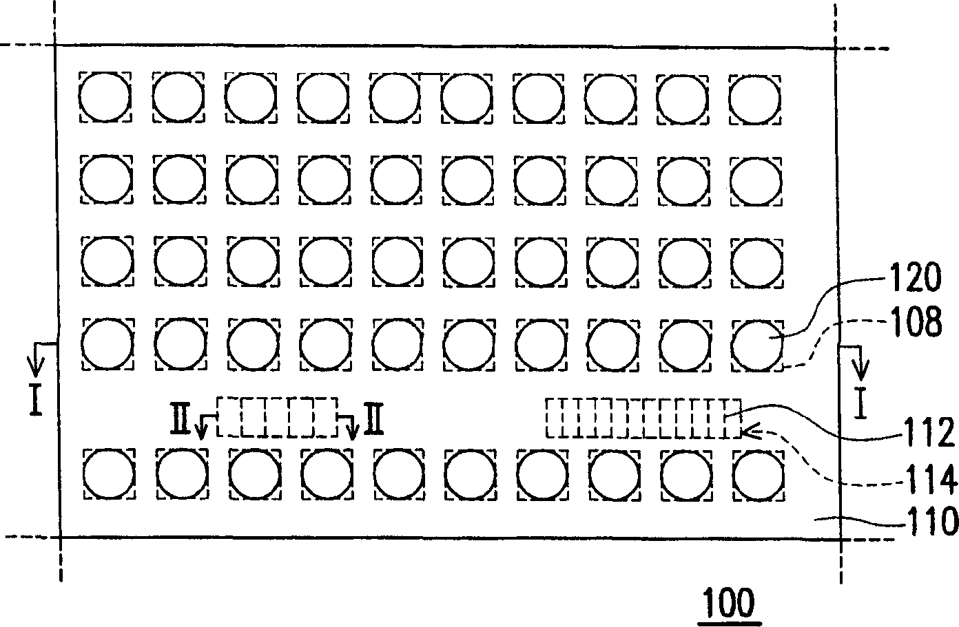
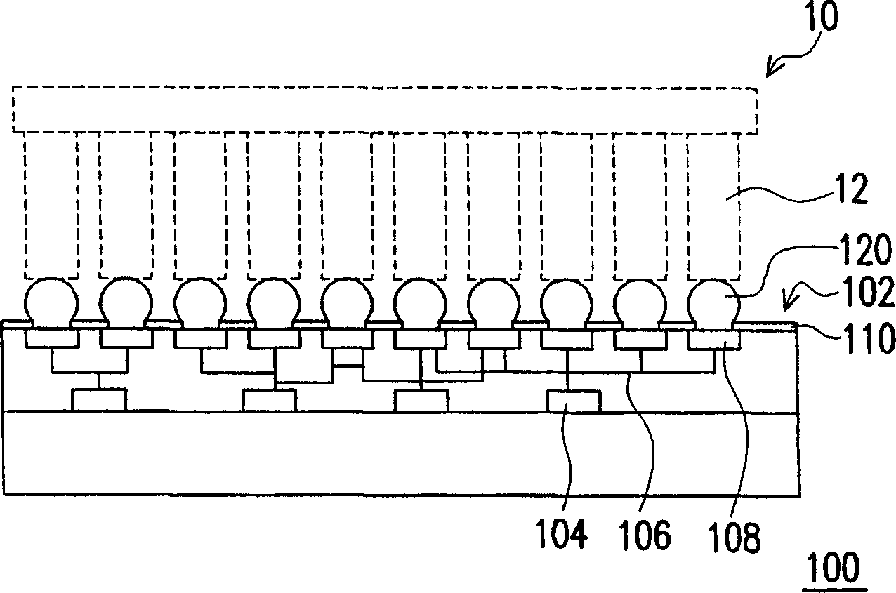
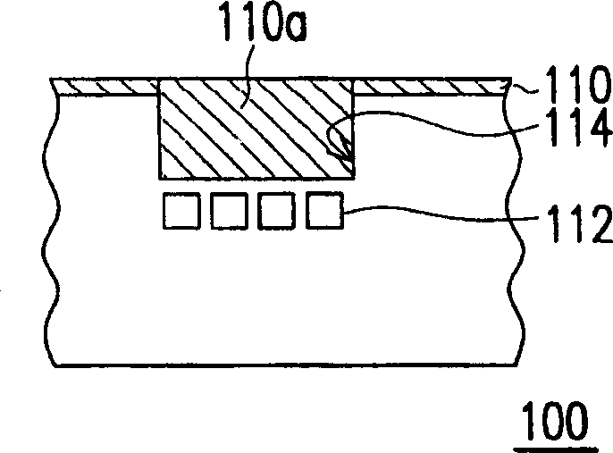
[0038] Please also refer to Figure 3A , 3B ,in Figure 3A A schematic partial top view of a wafer with test pads showing a preferred embodiment of the present invention, and Figure 3B show Figure 3A A schematic cross-sectional view along the I-I line. first as Figure 3A As shown, the active surface 202 of the chip 200 is configured with a plurality of flip-chip bonding pads 208 and a plurality of test pads 208a, and each flip-chip bonding pad 208 is electrically connected to the test pads, for example, via a trace 209 208 a , and these flip-chip bonding pads 208 are electrically connected to the active components 204 through metal interconnections 206 . It is worth noting that the test pad 208a is located at the periphery of the active surface 202, and the test pad 208a is completed when the flip-chip bonding pad 208 is made, and is used as a test contact point for the electrical state of the wafer 200, and the test pad 208a The area may be smaller than the area of ​...


PUM


Abstract

A wafer-class test and salient point technology and the chip structure with test pads are disclosed. The multiple test pads as the test points for analyzing and debugging the circuits are arranged on the active surface of wafer, and electrically connected with relative flip-chip welding pads of chip. The probe can directly contact the surface of test pads for testing the wafer. Based on the test result, it is determined that if the repair lines are cut off via repair window. Finally the protecting layer and salient points are sequentially generated on the active surface of wafer, which is the cut to form more chips.

Description

technical field [0001] The present invention relates to a testing and packaging process, and in particular to a wafer level testing and bumping process. Background technique [0002] With the rapid development of semiconductor technology and the increasing market demand for semiconductor-packaged products, more sophisticated and advanced semiconductor electronic components are constantly being developed. As far as the current semiconductor manufacturing and packaging and testing (packaging and testing) are concerned, after the integrated circuit (Integral Circuit, IC) design is completed, the front-end process of the semiconductor is carried out, which mainly includes the manufacturing and testing of the integrated circuit of the chip, etc., and then The chip (die) formed after wafer dicing is then, for example, wire bonded (wire bond) or flip chip bonded (flip chip bond), so that the chip's active surface (active surface) is flip chip bonded The bonding pads are electrical...

Claims


Application Information

Patent Timeline
IPC IPC(8): H01L21/28H01L21/60H01L21/66H01L21/768
CPCH01L2224/10
Inventor 余玉龙倪云鹏
Owner VIA TECH INC
Why Eureka
Try Eureka