Method for managing and allocating buffer storage during Ethernet interchange chip transmission of data

A technology for switching chips and data transmission, applied in transmission systems, digital transmission systems, data exchange networks, etc., can solve the problem of increasing the complexity of data processing and circuit design, the tight timing design of multicast reference count tables, and increasing the cost of switching chips, etc. problems, to achieve the effect of improving data processing, improving work reliability, and improving practicability

Inactive Publication Date: 2003-10-29
HUAWEI TECH CO LTD
View PDF0 Cites 31 Cited by
  • Summary
  • Abstract
  • Description
  • Claims
  • Application Information

AI Technical Summary

Problems solved by technology

[0016] 1. The number of visits to the multicast reference counting table is relatively large: in the whole process of data frame processing, the multicast reference counting table needs to be accessed in operations such as initialization, application for allocation, application for refresh, and application for release, which makes the multicast reference counting table The timing design of the counting table is very tight. In order to meet the processing speed requirements of the high-speed Ethernet switching chip, a relatively expensive and complicated circuit design scheme has to be adopted, which increases the cost of the switching chip.
[0017] 2. The processing of stacked speed data frames is inconsistent with that of ordinary data frames, which increases the complexity of data processing and circuit design

Method used


Image

  • Method for managing and allocating buffer storage during Ethernet interchange chip transmission of data
  • Method for managing and allocating buffer storage during Ethernet interchange chip transmission of data
  • Method for managing and allocating buffer storage during Ethernet interchange chip transmission of data

Examples


Embodiment Construction

[0033]Below according to accompanying drawing and embodiment the present invention will be described in further detail:

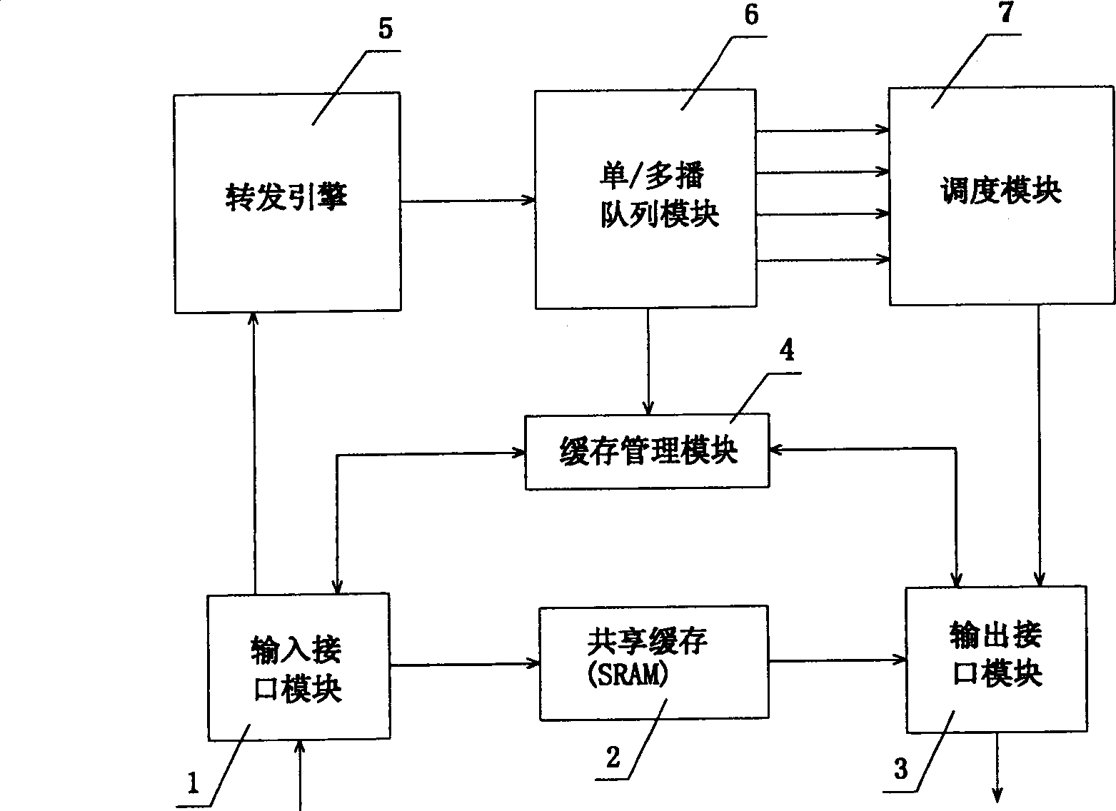
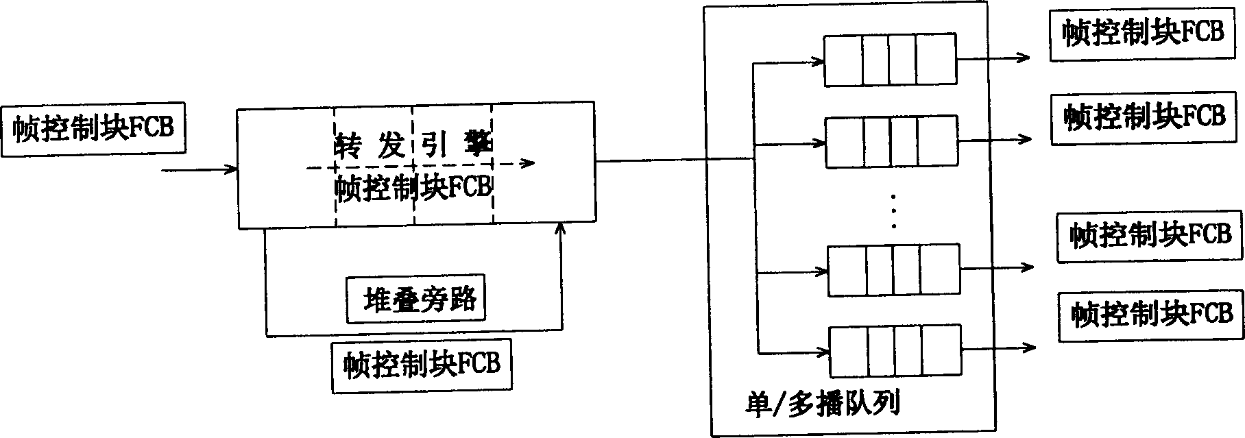
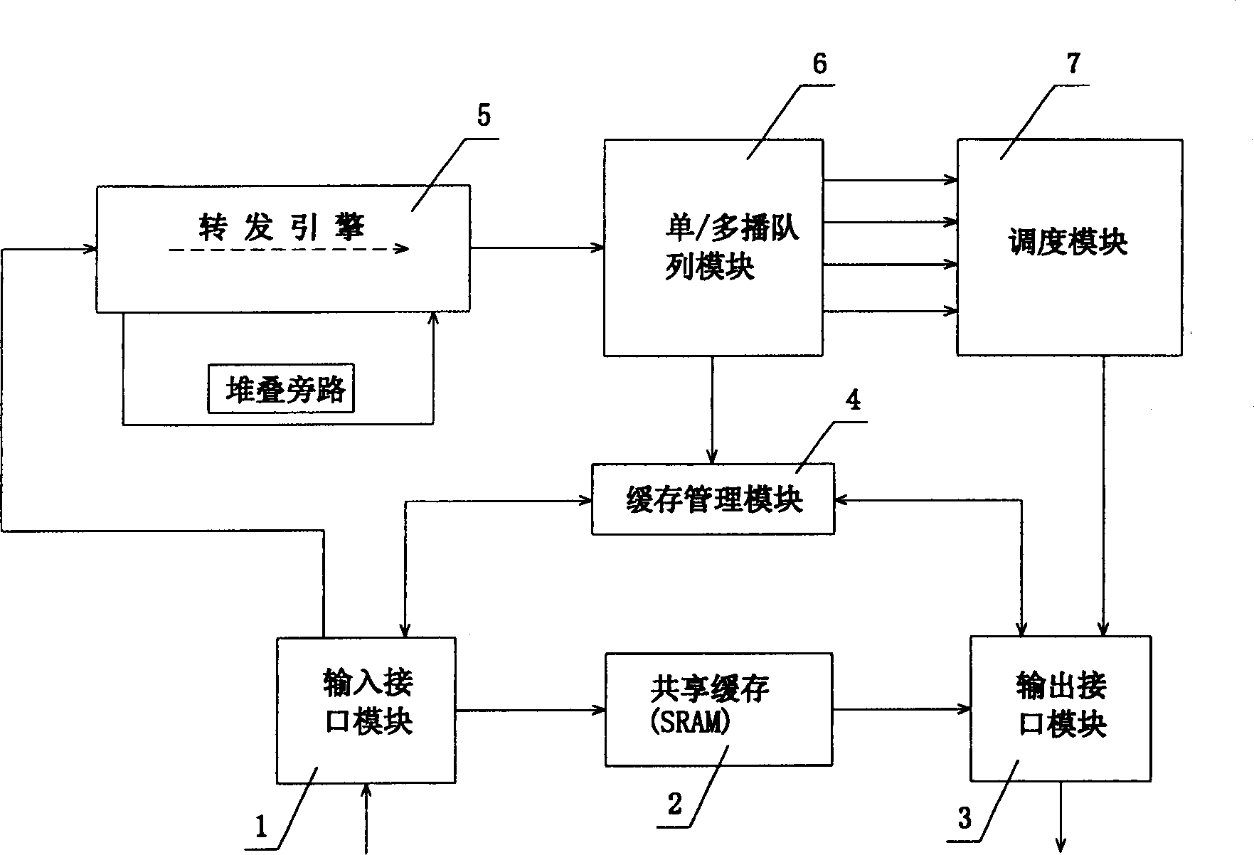
[0034] The number of ports provided with a switch chip is 27, such as image 3 As shown, a release weight table is used in the cache management module 4. The release weight table is a one-dimensional list, and each cache address pointer corresponds to one of the entries, and the value of the entry is the release value corresponding to the corresponding cache address pointer. The value of the weight, the shared cache has a total of 4K address pointers to maintain, each address pointer corresponds to a release weight table entry, the release weight table has a total of 4K entries, and the width of the entry is 5 bits. Using this cache management method The working process of the switch chip is as follows:

[0035] Such as image 3 As shown, when the switch chip is initialized, the initial value of each entry in the release weight table is set to 1FH, and th...


PUM


Abstract

A method for managing and allocating buffer in the data transmission procedure of Ethernet switch chip includes allocating the address pointer to input interface module by buffer management module, extracting control information by input interface module, combining it with address. In the buffer management module, there is a release weight table. Each address pointer is relative to a table item. Different release weight values are assigned to different frame control blocks. When frame control blocks are released, the release weight values are decreased until it is equal to zero, that is, all frames are processed.

Description

technical field [0001] The invention relates to electrical digital data processing, in particular to a method for managing and distributing buffers in the data transmission process of an Ethernet switch chip. Background technique [0002] A multi-port Ethernet switch chip that works in a store-and-forward mode first receives all Ethernet data frames that need to be forwarded from the external port and stores them in the shared buffer, and then reads the data frames from the shared buffer according to the forwarding requirements And send it to another external port, the shared cache can be designed inside the switch chip or placed outside the switch chip. [0003] In the existing data cache processing, such as figure 1 As shown, the Ethernet data frame entering the switch chip from the external port applies for caching to the cache management module at the input interface, and the cache management module feeds back a free cache address pointer to the input interface module a...

Claims


Application Information

Patent Timeline
Patent Type & Authority Applications(China)
IPC IPC(8): H04L12/24H04L12/28
Inventor 林郁林晖谭锐杨智明孙杰崔靖杰刘永志张志强饶伟年唐焰
Owner HUAWEI TECH CO LTD
Why Eureka
Try Eureka