
Method for manufacturing laminated electronic device

A technology for electronic devices and manufacturing methods, applied in the direction of multilayer capacitors, inductor/transformer/magnet manufacturing, chemical instruments and methods, etc., can solve the problems of harmful effects of conductive particles, easy intrusion into plating solution and flux, and low reliability.

Inactive Publication Date: 2004-01-14
MURATA MFG CO LTD
View PDF0 Cites 4 Cited by
  • Summary
  • Abstract
  • Description
  • Claims
  • Application Information

AI Technical Summary

Problems solved by technology

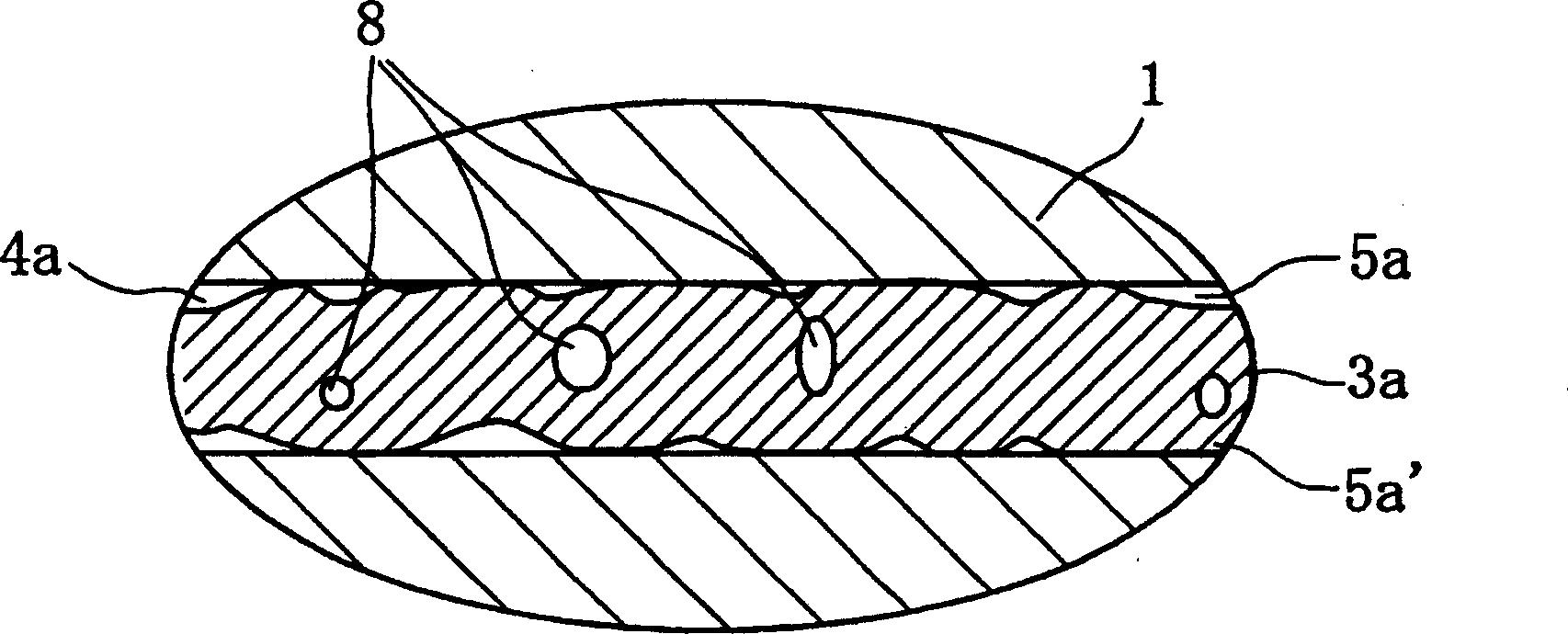
[0009] In addition, once the cross-sectional area ratio is reduced, the solvent will easily invade the plating solution and flux in order to expand the gap, and the components such as ions contained in these substances will have a harmful effect on the conductive particles, resulting in a problem of low reliability.

Method used


Image

  • Method for manufacturing laminated electronic device
  • Method for manufacturing laminated electronic device
  • Method for manufacturing laminated electronic device

Examples


Embodiment 1

[0077] The inventors first weighed NiO, CuO, ZnO, Fe in a predetermined amount 2 O 3 After waiting for the ferrite material, put these weighed objects into a ball mill containing PSZ (partially stabilized zirconia) with a diameter of 1 mm as a dispersion medium for wet mixing and pulverization to form a slurry powder. After the powder is separated from the PSZ, it is dried with a spray dryer and calcined at 650°C for 2 hours to form a calcined product.

[0078] Then the calcined product is added to the above ball mill to fully wet pulverize, and dried with a spray dryer to prepare calcined powder.

[0079] Then add polyvinyl butyral as a binder, dibutyl phthalate as a plasticizer, ammonium polycarboxylate as a dispersant, and toluene as a solvent to the calcined powder. After mixing with ethanol, it is made into ceramic slurry, which is further shaped into a sheet shape by a knife coating method or the like to prepare a magnet sheet (uncalcined ceramic sheet) with a thickness of 5...

Embodiment 2

[0088] Except that the Ag particle content in the conductive paste was 20% by volume and the resin particle content was 20% by volume, the multilayer inductor of Example 2 was produced according to the same method and procedure as Example 1. (Example 3)

Embodiment 3

[0089] Except that the content of Ag particles in the conductive paste was 26% by volume and the content of resin particles was 14% by volume, the multilayer inductor of Example 3 was produced according to the same method and procedure as Example 1. (Example 4)


PUM

PropertyMeasurementUnit
compressive strengthaaaaaaaaaa
particle sizeaaaaaaaaaa

Abstract

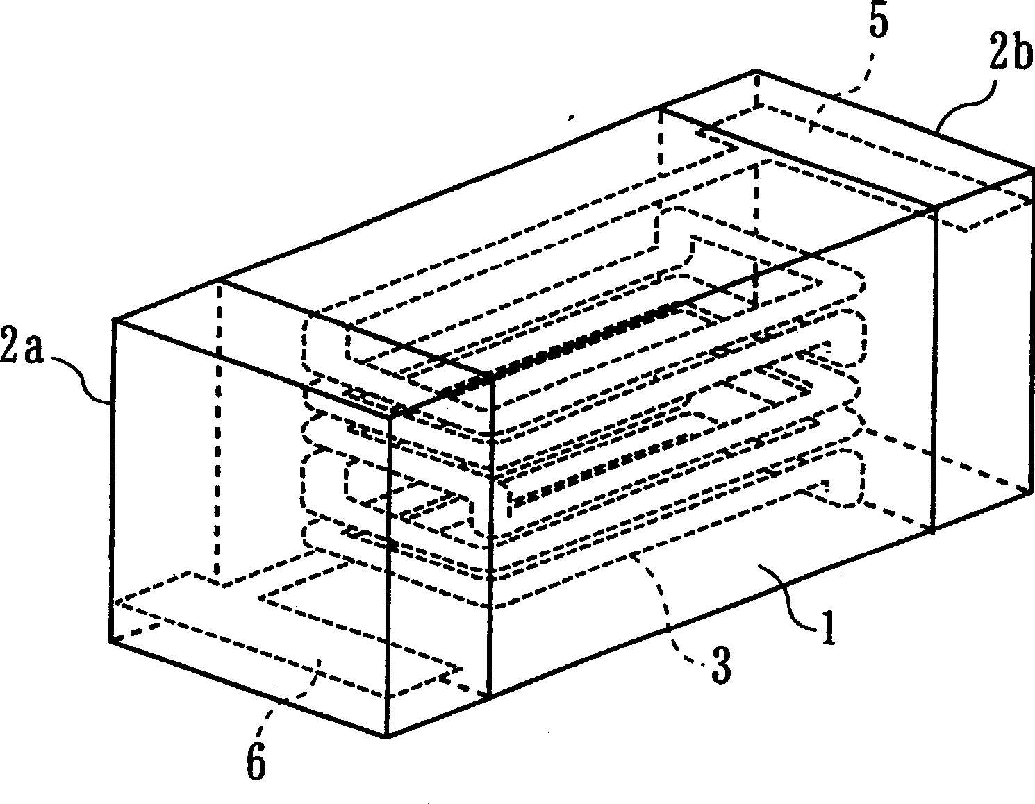
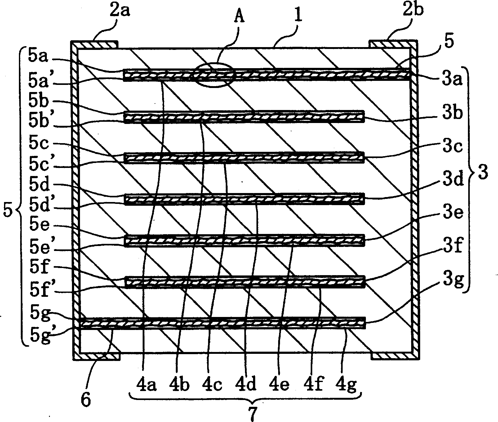
A method for producing a laminated electronic component.Conductive paste is prepared to contain conductive particles and resin particles having a thermal decomposition-ability. The resin particles have an average particle size of about 0.25 to about 1.50 times the average particle size of the conductive particles, The volume ratio of the resin particles is in the range of about 0.5 to about 1.0 the volume of the conductive particles, The conductive paste is applied to the surface of a ceramic layer to form a conductor layer. The ceramic layers and the conductor layers are alternately laminated. The laminate is fired to form a ceramic sintered laminate. Thus, a laminated electronic component is produced.

Description

Technical field [0001] The present invention relates to a method for manufacturing a laminated electronic device. In more detail, the present invention relates to a laminated body formed by laminating an unsintered ceramic layer and a conductor layer formed of a conductive paste to produce a ceramic sintered body. A method of manufacturing a laminated electronic device such as an inductor. Background technique [0002] Laminated ceramic electronic devices usually use a screen printing method to print a conductive paste (conductive paste) for internal electrodes on the surface of a thin unsintered ceramic layer to form a conductive pattern, and the ceramic sheets with the conductive pattern formed in this way are divided into a predetermined number After stacking to form a stacked body, the stacked body is subjected to a firing treatment, and then the external electrode is formed. [0003] However, in laminated ceramic electronic devices, the thermal expansion coefficient and shri...

Claims


Application Information

Patent Timeline
Patent Type & Authority Applications(China)
IPC IPC(8): H01G4/232C04B35/26H01B1/22H01F17/00H01F41/04H01G4/008H01G4/012H01G4/30H05K1/09
CPCC04B35/62655C04B2235/3281H01G4/30C04B2235/3284B32B2311/08H01B1/22B32B2309/022C04B2237/704H01F17/0013C04B35/265H01F2017/048H01G4/008C04B35/6264H01F41/046C04B2235/3279C04B2235/96H05K1/092C04B2237/408C04B2237/34H01G4/012B32B18/00H01F41/00
Inventor 河野上正晴穴太公治
Owner MURATA MFG CO LTD
Features
  • Generate Ideas
  • Intellectual Property
  • Life Sciences
  • Materials
  • Tech Scout
  • Unparalleled Data Quality
  • Higher Quality Content
  • 60% Fewer Hallucinations
Learn More