Apparatus for compensatnig deviation of test temperature is semiconductor device processing machine

A technology of semiconductors and processors, applied in the field of processors, can solve the problems of lower yield and reliability

Inactive Publication Date: 2004-01-28
MIRAE CORPORATION
View PDF0 Cites 22 Cited by
  • Summary
  • Abstract
  • Description
  • Claims
  • Application Information

AI Technical Summary

Problems solved by technology

This results in reduced yield and reliability due to not being able to test at the exact temperature desired or within the desired temperature range

Method used


Image

  • Apparatus for compensatnig deviation of test temperature is semiconductor device processing machine
  • Apparatus for compensatnig deviation of test temperature is semiconductor device processing machine
  • Apparatus for compensatnig deviation of test temperature is semiconductor device processing machine

Examples


Embodiment Construction

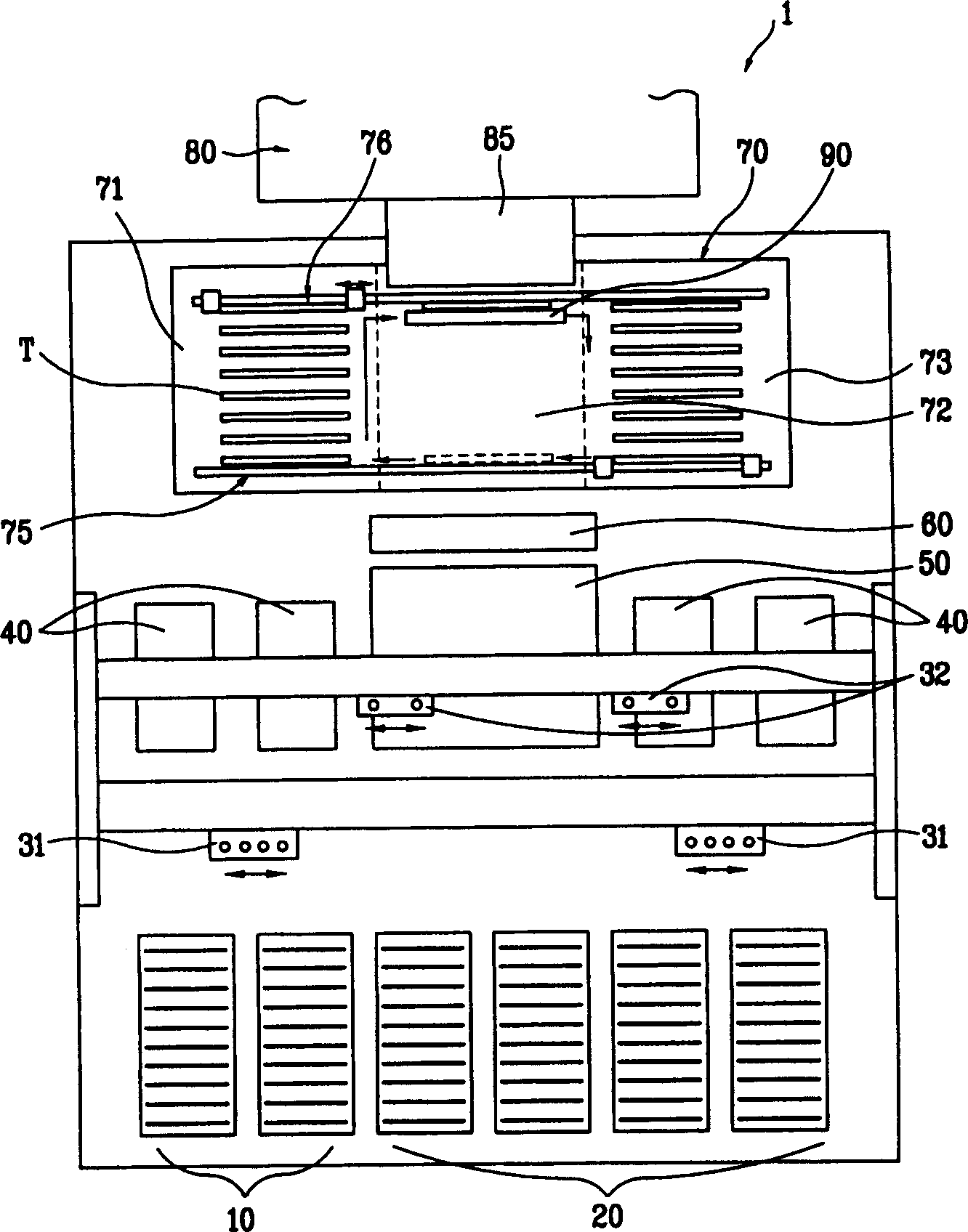
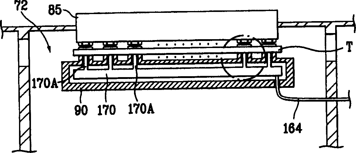
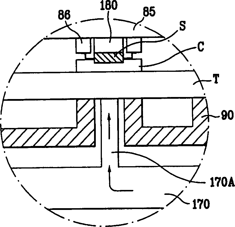
[0024] Reference will now be made in detail to embodiments and examples of the invention illustrated in the accompanying drawings. figure 1 is a schematic plan view of a handler according to the invention with means for compensating test temperature deviations. Figure 2 is figure 1 Side cutaway view of the test location of the handler shown.

[0025] The processor and how it works are described below.

[0026] figure 1 The shown handler includes a loading unit 10 at the front of the handler 1, into which user trays can be loaded, and an unloading unit 20 at one side of the loading unit 10, in which semiconductor devices under test can be loaded on the user trays , and classify the tested semiconductor devices according to the test results.

[0027] Buffer units 40 are provided on both sides of a middle position of the handler 1 and temporarily store semiconductor devices transferred from the loading unit 10 . The exchange unit 50 is provided between the buffer units 40 . ...


PUM


Abstract

A semiconductor device handler is provided, wherein a test temperature deviation of a semiconductor device caused by heat produced by the semiconductor device itself during testing is compensated for, allowing a test of the semiconductor device to be carried out at an exact temperature, or within an exact temperature range. The semiconductor device handler comprises at least one enclosed chamber, a heating / cooling apparatus configured to bring an inside of the at least one chamber to a low or high temperature state, a pushing unit provided within the at least one chamber and configured to push a plurality of semiconductor devices mounted on a test tray into test sockets of a test board located within the at least one chamber for testing, a cooling fluid supplying apparatus configured to supply cooling fluid, a nozzle assembly configured to spray cooling fluid received from the cooling fluid supplying apparatus onto the semiconductor devices fitted to the test sockets, and a control unit configured to control spraying of cooling fluid onto the semiconductor devices during testing to compensate for temperature changes of the semiconductor devices that occur during testing.

Description

technical field [0001] The present invention relates to a handler for testing semiconductor devices, and more particularly to a device for compensating test temperature deviations in a semiconductor device handler. Background technique [0002] In general, memory or non-memory semiconductor devices, or components each having memory and / or non-memory semiconductor devices disposed on a substrate to form circuits, are subjected to various tests after manufacture and before shipment. A semiconductor device handler (hereinafter simply referred to as "handler") is a device used to automatically transfer semiconductor devices or components during testing. The program executed inside the handler is that when the loader and stacker receives a tray with semiconductor devices or components therein, the picking manipulator transports the semiconductor devices or components to be tested to the test position, installs them into the test sockets, and executes the required For the test, t...

Claims


Application Information

Patent Timeline
Patent Type & Authority Applications(China)
IPC IPC(8): G01R31/26G01R1/44G01R31/28
CPCG01R31/2877G01R31/2867G01R31/2862
Inventor 宋在明咸哲镐朴赞毫黄义星林祐永徐载奉李应龙李炳基
Owner MIRAE CORPORATION
Why Eureka
Try Eureka