

Method of forming metal wire of LCD device
A device and metal layer technology, applied in the field of liquid crystal display devices, can solve the problems of complicated reprocessing, failure of reprocessing of LCD devices, etc.
- Summary
- Abstract
- Description
- Claims
- Application Information
AI Technical Summary
Problems solved by technology
Method used
Image

Examples
Embodiment Construction
[0039] Preferred embodiments of the invention will be described in detail with reference to the examples in the accompanying drawings.
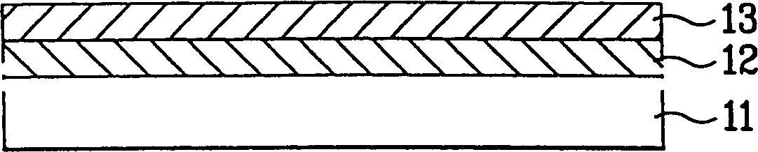
[0040] Figure 3A is an exemplary cross-sectional view illustrating a method of forming lines of an LCD device according to the present invention. Such as Figure 3A As shown in , an aluminum (pure aluminum) Al layer 22 or an aluminum alloy (AlNd) layer 22 and a molybdenum Mo layer 23 are deposited on a glass substrate 21 in sequence. In this example, the aluminum Al layer 22 may be formed in a thickness of 10 Å to 3000 Å, and the molybdenum Mo layer 23 may be formed in a thickness of 10 Å to 2000 Å.
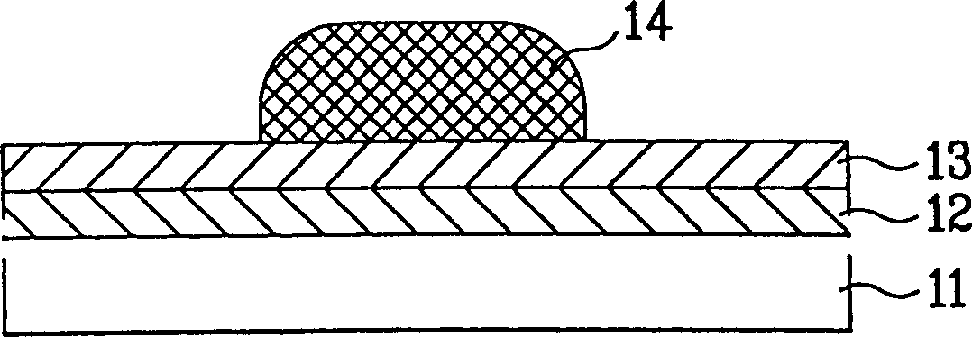
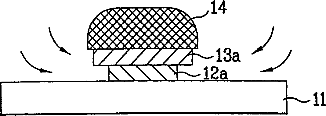
[0041] Figure 3B is an exemplary cross-sectional view illustrating a method of forming lines of an LCD device according to the present invention. Such as Figure 3B As shown in , a photoresist layer can be deposited on the entire surface of the molybdenum Mo layer 23, and a mask (not shown) is used to perform exposure and development proces...
PUM
 Abstract
Description
Claims
Application Information