Reading circuit and semiconductor memory device including same

A technology for reading circuits and storage devices, which is applied in the field of reading circuits, and can solve the problems that the pre-charging circuit has no power supply capability, the bit line cannot be charged, and it is difficult to shorten the reading time.

Inactive Publication Date: 2004-03-24
SAMSUNG ELECTRONICS CO LTD
View PDF1 Cites 19 Cited by
  • Summary
  • Abstract
  • Description
  • Claims
  • Application Information

AI Technical Summary

Problems solved by technology

Therefore, the precharge circuit 109 has little power supply capability, and the bit line cannot be charged to a level higher than the clamping potential set by the feedback bias circuit 103A.
[0064] As described above, even if the clamp potential of the bit line is set by the feedback bias circuit 103A and quickly charged by the precharge circuit 109, it is still difficult to shorten the reading time.

Method used


Image

  • Reading circuit and semiconductor memory device including same
  • Reading circuit and semiconductor memory device including same
  • Reading circuit and semiconductor memory device including same

Examples


Embodiment Construction

[0108] Hereinafter, the semiconductor memory device according to the present invention will be described by way of descriptive examples with reference to the accompanying drawings.

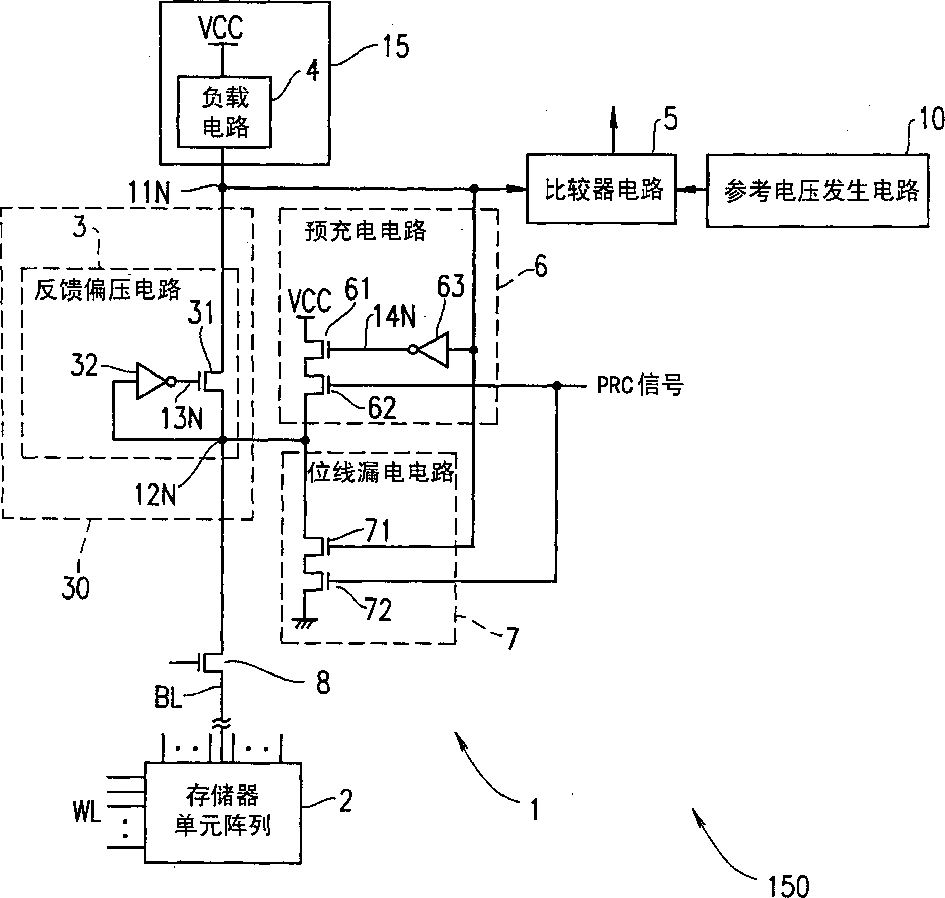
[0109] figure 1 is a block diagram illustrating a partial structure of the semiconductor memory device 150 according to an example of the present invention.

[0110] The semiconductor memory device 150 includes: a memory cell array 2 including a plurality of memory cells; and a reading circuit 1 for reading a selected memory cell among the plurality of memory cells stored in the memory cell array 2 (reading memory cell ) in the information.

[0111] The read circuit 1 comprises: a current source circuit 15, which is used to provide current to the bit line BL connected to the read memory cell; a comparator circuit 5, which is used as a comparison circuit; a pre-charge circuit 6, which is used as a charging circuit; a disconnection circuit 30, used to electrically disconnect the comparator circui...


PUM


Abstract

A reading circuit for reading information stored in a memory cell includes a current supply circuit for supplying a current to a bit line connected to the memory cell; a comparison circuit for comparing a potential of the bit line supplied with the current by the current supply circuit with a reference potential so as to output the information stored in the memory cell; a disconnection circuit for electrically disconnecting the comparison circuit and the memory cell from each other under a prescribed condition; a charge circuit for charging the bit line, the charge circuit stopping charging of the bit line when the potential of the bit line exceeds a prescribed potential; and a discharge circuit for discharging the bit line when the potential of the bit line exceeds the prescribed potential.

Description

technical field [0001] The present invention relates to a readout circuit and a semiconductor memory device including the readout circuit. Background technique [0002] Conventionally, various types of electrically writable nonvolatile memories have been proposed, including, for example, EEPROM (Electrically Erasable Programmable Read Only Memory), flash EEPROM (hereinafter, also referred to as "flash memory"), MRAM (Magnetic Random Access Memory) and OUM (Oversinski Effect Unified Memory). [0003] These types of non-volatile memories have in common that data is stored in and read from memory cells, but have different structures. [0004] For example, a flash memory uses a MOSFET (Metal Oxide Semiconductor Field Effect Transistor, also referred to as a “transistor”) having a floating gate as a memory cell. In flash memory, charge is accumulated in the floating gate of the memory cell. According to the amount of charge accumulated in the floating gate, the threshold volta...

Claims


Application Information

Patent Timeline
Patent Type & Authority Applications(China)
IPC IPC(8): G11C16/06G11C7/06G11C11/15G11C11/16G11C16/00G11C16/28
CPCG11C11/16G11C7/062G11C16/28G11C7/067G11C16/00
Inventor 森川佳直
Owner SAMSUNG ELECTRONICS CO LTD
Why Eureka
Try Eureka