Storage circuit, displaying circuit and displaying device

A technology for storage circuits and display devices, which is applied to the storage circuits for storing pixel data signals, display devices, and display circuits. It can solve problems such as the decrease in resistivity of liquid crystal materials and the deterioration of liquid crystal material quality, and reduce power dissipation. Effect of preventing deterioration

Inactive Publication Date: 2004-04-21
ADVANCED LCD TECH DEVMENT CENT
View PDF0 Cites 7 Cited by
  • Summary
  • Abstract
  • Description
  • Claims
  • Application Information

AI Technical Summary

Problems solved by technology

For liquid crystal display devices, applying a voltage of one polarity to the liquid crystal layer for a long period of time may lead to deterioration of the quality of the liquid crystal material
For example, the resistivity of liquid crystal materials may drop

Method used


Image

  • Storage circuit, displaying circuit and displaying device
  • Storage circuit, displaying circuit and displaying device
  • Storage circuit, displaying circuit and displaying device

Examples


Embodiment Construction

[0025] A liquid crystal display device according to an embodiment of the present invention will now be described with reference to the drawings.

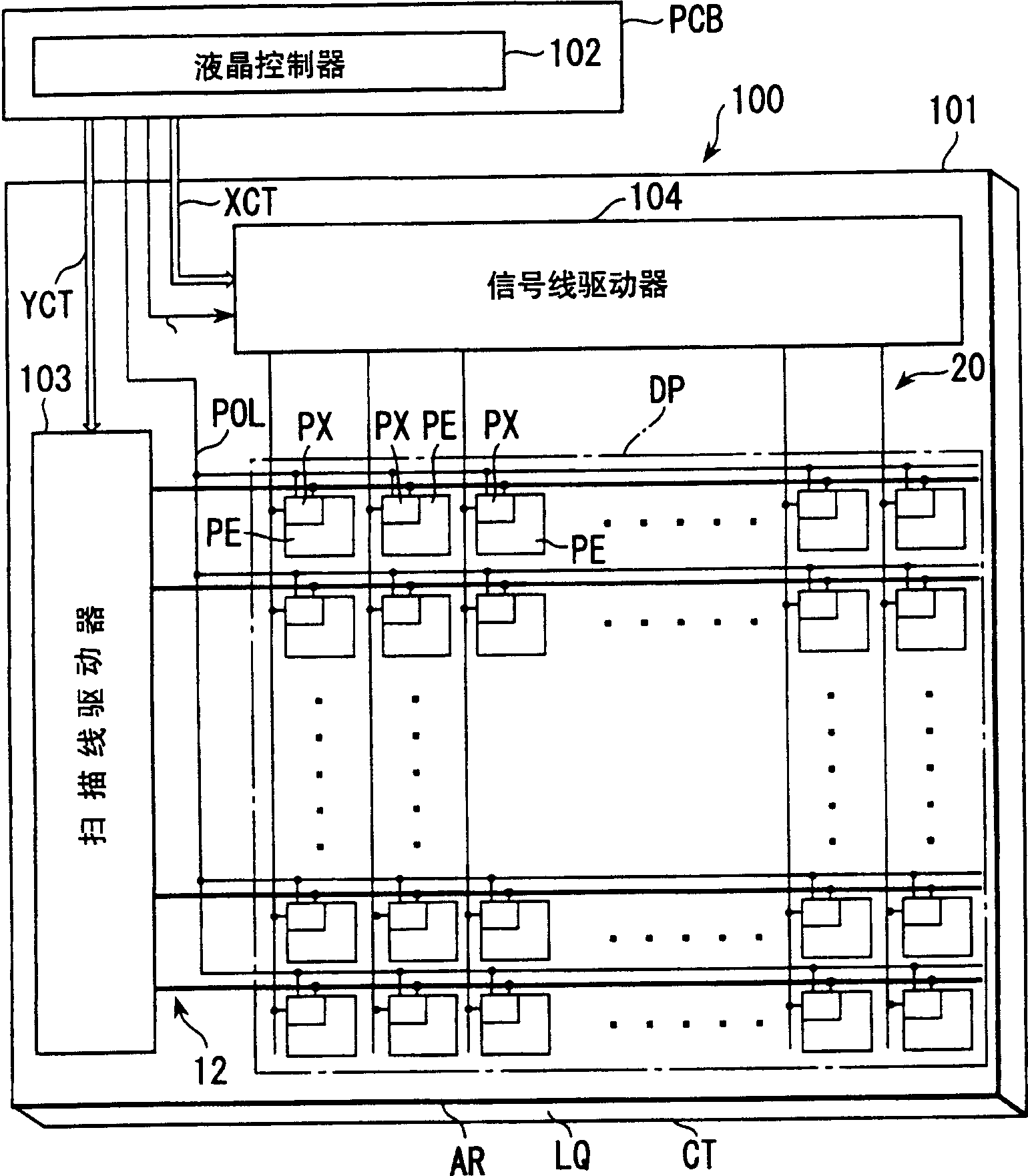
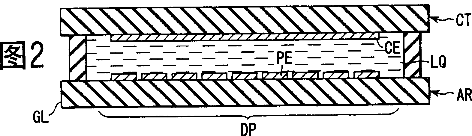
[0026] figure 1 A schematic circuit configuration of the liquid crystal display device 100 is shown, and FIG. 2 shows a schematic cross-sectional structure of the liquid crystal display device 100 .

[0027] The liquid crystal display device 100 includes a liquid crystal display panel 101 and a liquid crystal controller 102 for controlling the liquid crystal display panel 101 . In the structure of the liquid crystal display panel 101, a liquid crystal layer LQ is held between an array substrate AR and a counter substrate CT. The liquid crystal controller 102 is located on the driving circuit board PCB independent of the liquid crystal display panel 101 .

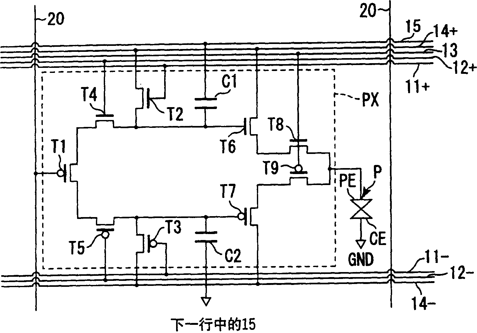
[0028] The array substrate AR includes a plurality of pixel electrodes PE arranged in a multi-row and multi-column matrix in the display area DP on the glass plate GL, a plurali...


PUM


Abstract

A liquid crystal display includes pixels arrayed in a matrix of rows and columns, scanning lines extending along the rows of the pixels, signal lines extending along the columns of the pixels, and pixel driving sections which are disposed near intersections of the scanning lines and signal lines, and each of which is controlled via one scanning line to capture a data signal on one signal line and output the data signal to one pixel. Particularly, each pixel driving section includes a memory circuit having a transistor whose gate is connected to the one signal line, and first and second storage capacitances which are charged to positive and negative power supply voltages and connected to a source and drain of the transistor to store the data signal as analog drive voltages of positive and negative polarities, respectively.

Description

technical field [0001] The present invention generally relates to a display device such as a liquid crystal display device or an EL (Electro Luminescence) display device, and more particularly, the present invention relates to a memory circuit, a display circuit, and a display device such as for storing pixel data signals. Background technique [0002] In a liquid crystal display device, a large number of pixels are arranged in a matrix of rows and columns to display an image corresponding to one frame of a video signal input from an external signal source such as a personal computer. The video signal is serially and parallel-converted into a data signal, and the data signal is applied to the pixels in each row as an analog driving voltage. When the video signal is in digital form, a digital-to-analog converter (DAC) is used to obtain the data signal. These data signals are applied to pixels in each row through signal lines. The capacitance of each pixel is charged or disc...

Claims


Application Information

Patent Timeline
Patent Type & Authority Applications(China)
IPC IPC(8): G02F1/133G09G3/36
CPCG09G2300/0842G09G3/3648G09G2300/0809G09G3/3614G02F1/133
Inventor 松村正清是成贵弘
Owner ADVANCED LCD TECH DEVMENT CENT
Why Eureka
Try Eureka