High-efficiency high-brightness multiple active district tunnel reclaimed white light light emitting diodes

A light-emitting diode, high-brightness technology, applied in electrical components, circuits, semiconductor devices, etc., can solve the problems of low absorption rate of phosphor powder, short life of phosphor powder, low color rendering index, etc., and achieve high luminous efficiency and improved quantum efficiency , Chroma realistic effect

Inactive Publication Date: 2004-04-21
BEIJING TIMESLED TECH CO LTD
View PDF0 Cites 30 Cited by
  • Summary
  • Abstract
  • Description
  • Claims
  • Application Information

AI Technical Summary

Problems solved by technology

The biggest disadvantage of this type of white light-emitting diode is its halo effect: the bypass viewing angle is multi-colored and non-white; secondly, the low absorption rate of phosphor powder leads to low luminous efficiency and low color rendering index (CRI); at the same time, it is difficult to package and compared with semiconductor materials. Phosphors suffer from short lifetime and poor reliability

Method used


Image

  • High-efficiency high-brightness multiple active district tunnel reclaimed white light light emitting diodes
  • High-efficiency high-brightness multiple active district tunnel reclaimed white light light emitting diodes
  • High-efficiency high-brightness multiple active district tunnel reclaimed white light light emitting diodes

Examples


Embodiment 1

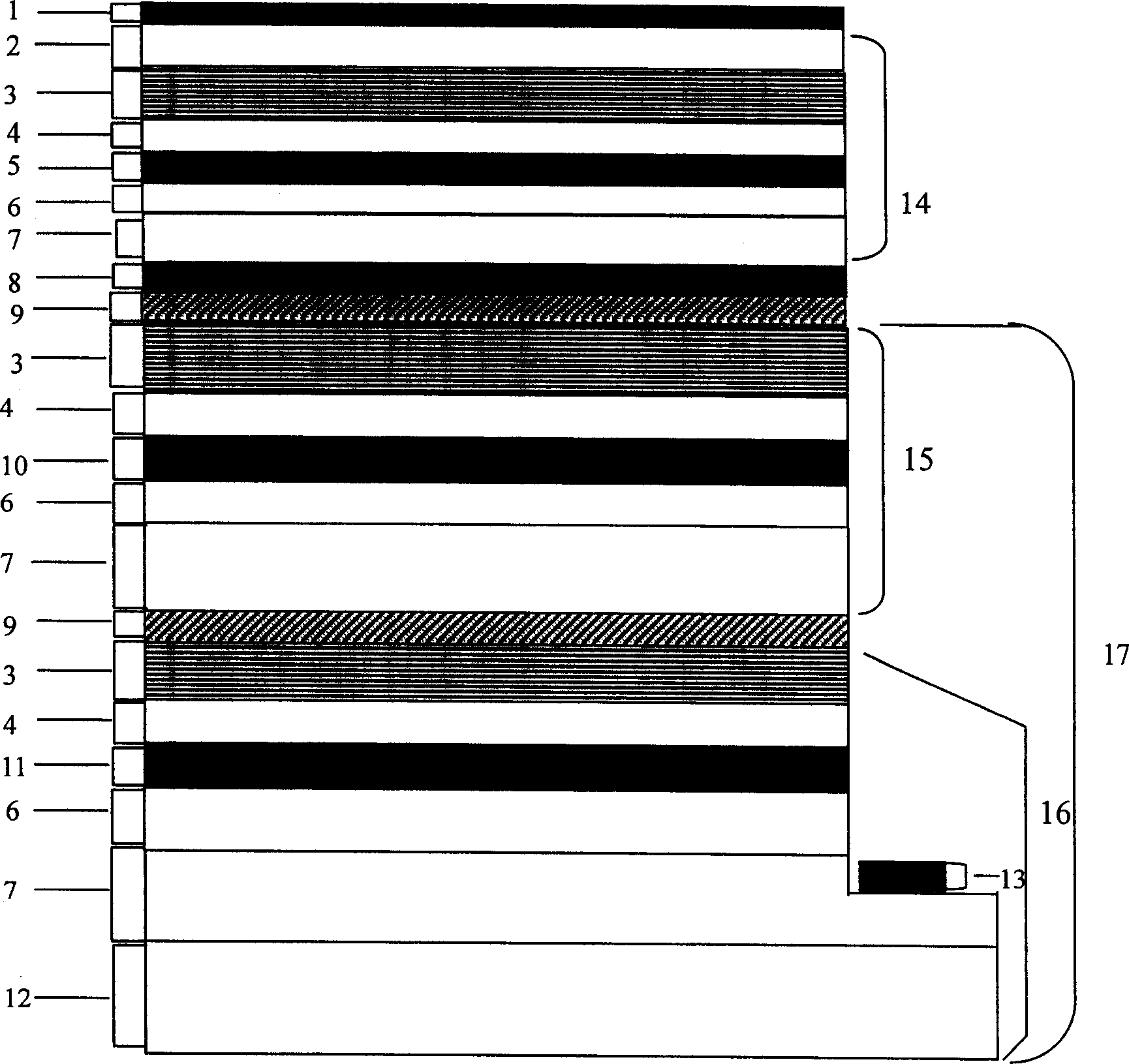
[0036] Such as Figure 7 Shown, its preparation process and method are as follows:

[0037] 1. Use common MOVCD method in N + - On the GaAs substrate, epitaxially grow N++GaAs / P++GaAs tunnel junction 9, N-GaInP transition layer 7, N-AlInP lower confinement layer 6, AlGaInP / GaInP heterojunction light-emitting region 5, and P-AlInP top Confinement layer 4, p+GaAs contact layer 2. Then, the red light-emitting unit 14 is obtained by evaporating or sputtering the p-type metal electrode Ti / Au (1) on the front side, and then removing the substrate GaAs through a grinding and thinning process;

[0038]2. On the sapphire or SiC substrate, grow n-GaN transition layer 7, n-InGaN lower confinement layer 6, InGaN / GaN multi-quantum well blue light emitting region 11, p-AlGaN upper confinement layer 4, AlInN / GaN DBR Blue light reflection layer 3, n++InGaN / P++GaN tunnel junction 9, n-GaN transition layer 7, n-InGaN lower confinement layer 6, InGaN / GaN multi-quantum well green light emittin...

Embodiment 2

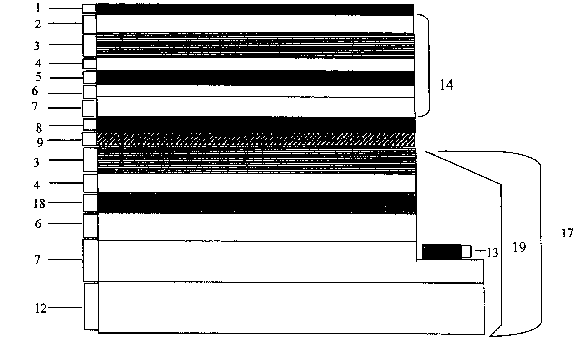
[0041] Such as Figure 8 Shown, its preparation process and method are as follows:

[0042] 1. Use common MOVCD method in N + - On the GaAs substrate, epitaxially grow N++GaAs / P++GaAs tunnel junction 9, N-GaInP transition layer 7, N-AlInP lower confinement layer 8, AlGaInP / GaInP heterojunction light-emitting region 5, and P-AlInP top Confinement layer 4, p+GaAs contact layer 2. Then, the red light-emitting unit 14 is obtained by evaporating or sputtering the p-type metal electrode Ti / Au (1) on the front side, and then removing the substrate GaAs through a grinding and thinning process;

[0043] 2. On a sapphire or SiC substrate, grow n-GaN buffer layer 7, n-InGaN lower confinement layer 6, InGaN / GaN multi-quantum well blue-green light-emitting region 18, p-AlGaN upper confinement layer 4, AlInN / GaN DBR blue light reflection layer 3, P++GaN contact layer 2, evaporate n-type electrode 13 after photolithography and etching to form a combination of blue and green light emittin...


PUM


Abstract

The high efficiency high brightness multi active area tunnel regeneration white light LED. This invention includes: ordinate-lead overlapped P type electrode (1), red light emission unit (14), tunnel junction (9), underlayer chip (17) consisted of green light emission unit(19), blue light emission, and tunnel junction or blue-green light emission, n type electrode (13), chip bonding layer (8) set between the red light emission unit and tunnel junction next to it or underlayer chip (17) and tunnel junction next to it. This invention adopts the semiconductor material, comparing with the fluorescence device it has high reliability, long useful life, chrominance reality.

Description

technical field [0001] The utility model relates to a high-efficiency, high-brightness multi-active area tunnel regenerative white light semiconductor light-emitting diode (LED), which belongs to the technical field of semiconductor optoelectronics and relates to a light-emitting diode. Background technique [0002] The current traditional white light semiconductor light-emitting diode design method and its existing problems: [0003] 1. Multiple high-brightness traditional red, green, and blue three-primary light-emitting diodes, such as image 3 with 4 As shown, the planar distribution of white light-emitting diodes that make up pixel lights, such as Figure 5 As shown, the emitted color changes according to the different power controls added to each chip, and white illumination sources with different brightness can be emitted. The disadvantages of this white light emitting diode are high cost, poor resolution, poor spatial directionality of chromaticity, and the driving...

Claims


Application Information

Patent Timeline
Patent Type & Authority Applications(China)
IPC IPC(8): H01L29/08H01L33/00H01L33/08
CPCH01L33/0016H01L33/08
Inventor 沈光地郭霞郭伟玲高国廉鹏门伟钢李建军邹德恕陈建新
Owner BEIJING TIMESLED TECH CO LTD
Why Eureka
Try Eureka