
Electronic circuit, modulating method, information processing devcie and information processing method

An electronic circuit and amplitude modulation technology, applied in the direction of modulation, amplitude modulation of semiconductor devices with at least 3 electrodes, amplitude modulation, etc., can solve problems such as communication failures and data distortion, and achieve the effect of reducing the number of times

Inactive Publication Date: 2004-05-19
SONY CORP
View PDF2 Cites 7 Cited by
  • Summary
  • Abstract
  • Description
  • Claims
  • Application Information

AI Technical Summary

Problems solved by technology

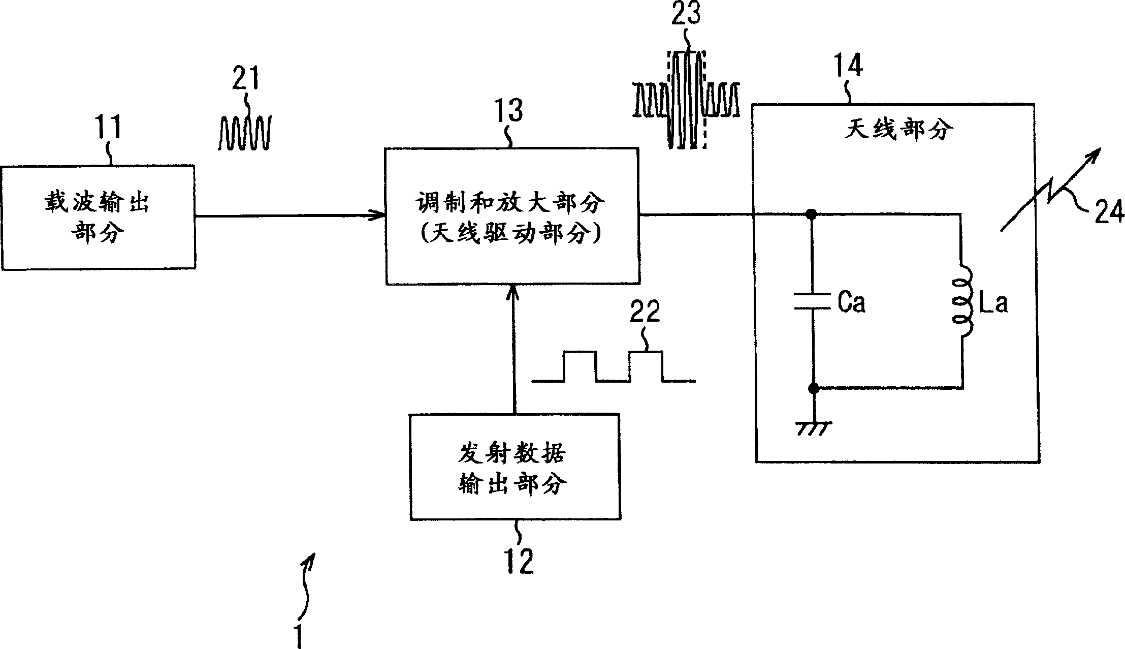
[0019] However, when following the above operations from figure 2 When the electromagnetic wave 24 (corresponding to the digital data of the pulse signal 22 superimposed on the carrier wave 21) emitted by the antenna part 14 of the transmitting device 1 is received and demodulated by an IC card having a limiter for limiting the input, when the limiter The demodulated data is distorted within the operating range of the transmitter, and as a result, there is a problem that communication failures often occur

Method used


Image

  • Electronic circuit, modulating method, information processing devcie and information processing method
  • Electronic circuit, modulating method, information processing devcie and information processing method
  • Electronic circuit, modulating method, information processing devcie and information processing method

Examples


Embodiment Construction

[0062] The applicant of the present application has analyzed the causes of the above-mentioned conventional problems, and devised the present invention based on the analysis results. Therefore, first, the analysis results, that is, the causes of the above-mentioned conventional problems will be introduced.

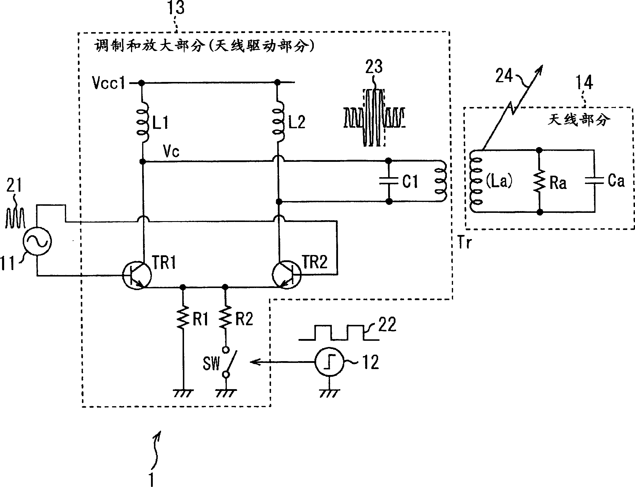
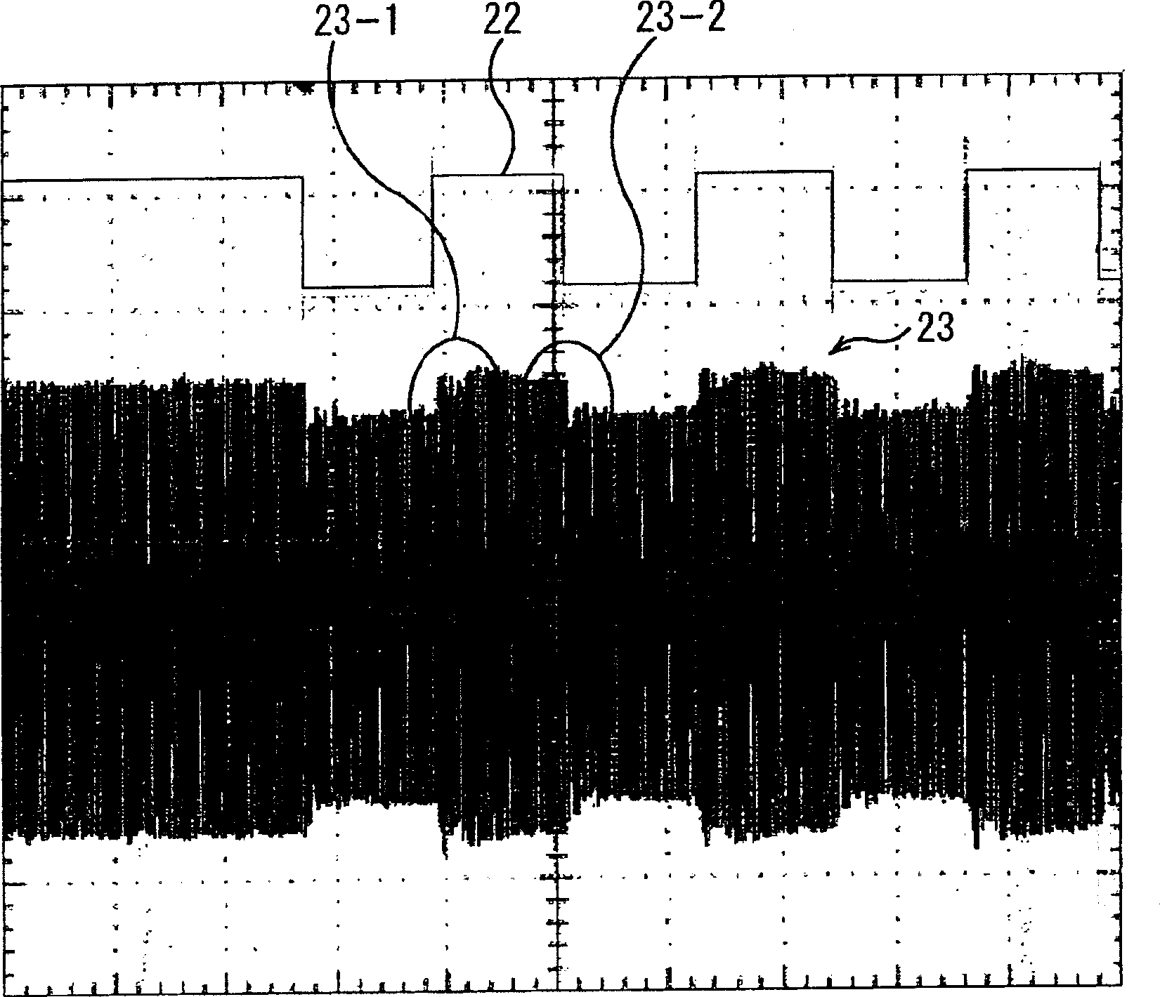
[0063] by using figure 2 The applicant of the present application measured the collector voltage Vc (amplitude modulation wave 23) and the magnetic flux (electromagnetic wave) 24 output from the antenna section 14 under the condition that the pulse signal 22 is actually input from the transmission data output section 12. exist image 3 with 4 The measurement results are shown in . which is, image 3 shown in figure 2 The measurement diagram of pulse signal 22 and collector voltage Vc (amplitude modulation wave 23) in the transmitting device 1 of the present invention, Figure 4 A pulse signal 22 and a magnetic flux (electromagnetic wave) 24 output from the antenna ...


PUM


Abstract

A shaped-wave application section inputs a first pulse signal corresponding to transmission data output from a transmission data output section, and applies, to a modulation and amplification section, a signal wave corresponding to a second pulse signal such that the waveform of the first pulse signal is shaped. The pulse signal applied to the base of the transistor of the modulation and amplification section is amplitude-modulated into an amplitude-modulated wave in which the amplitude-modulated portion is strengthened, in accordance with the signal wave corresponding to the second pulse signal applied to the emitter thereof. The amplitude-modulated wave is supplied to an antenna section including a resonance circuit via the collector thereof, and is transmitted as an electromagnetic wave from the antenna section.

Description

technical field [0001] The present invention relates to an electronic circuit, a modulation method, an information processing device, and an information processing method. More specifically, the present invention relates to an electronic circuit in which the number of occurrences of communication failures at the receiving end is reduced when data is transmitted through an antenna including a resonant circuit in an amplitude modulation manner, the present invention also relates to its modulation method, its information processing device and its information processing methods. Background technique [0002] An IC (Integrated Circuit) card system employing a non-contact communication technique is composed of a portable IC card and a device generally called a card reader / writer (hereinafter referred to as "R / W device"). The R / W device reads out information stored in the IC card in a non-contact manner and is capable of storing predetermined information in the IC card in a non-co...

Claims


Application Information

Patent Timeline
Patent Type & Authority Applications(China)
IPC IPC(8): H03C1/00H03C1/36H03C1/44H04B1/59H04L27/02H04L27/04H04L27/36
CPCH04L27/04H04L27/367H03C1/36
Inventor 前田龙男山形昭彦
Owner SONY CORP
Learn More