SOI wafer and its manufacturing method
A manufacturing method and wafer technology, applied in the fields of semiconductor/solid-state device manufacturing, electrical components, electrical solid-state devices, etc., can solve problems such as the influence of device yield rate, and achieve the goal of reducing device defects, improving device yield rate, and reducing LPD defect density. Effect
- Summary
- Abstract
- Description
- Claims
- Application Information
AI Technical Summary
Problems solved by technology
Method used
Image

Examples
Embodiment Construction
[0020] The present invention will be described in detail below.
[0021] In order to produce an SOI wafer that suppresses the generation of SOI islands that occur during lift-off or reduces the density of LPD defects that exist on the surface of the SOI wafer, the inventors of the present application found that As long as the implantation amount of hydrogen ions or rare gas ions is controlled within a predetermined range, the present invention has been accomplished by examining various conditions.
[0022] SOI islands with a certain width can be observed after the lift-off heat treatment at the platform portion where the substrate surface is exposed at the edge of the SOI wafer. Furthermore, the peeling by the ion implantation peeling method may be caused by the growth of defects caused by hydrogen or rare gas generated in the peeling heat treatment, and the force of rapid volume expansion caused by the gasification of implanted hydrogen or rare gas, The main reason for this ...
PUM
| Property | Measurement | Unit |
|---|---|---|
| size | aaaaa | aaaaa |
| electrical resistivity | aaaaa | aaaaa |
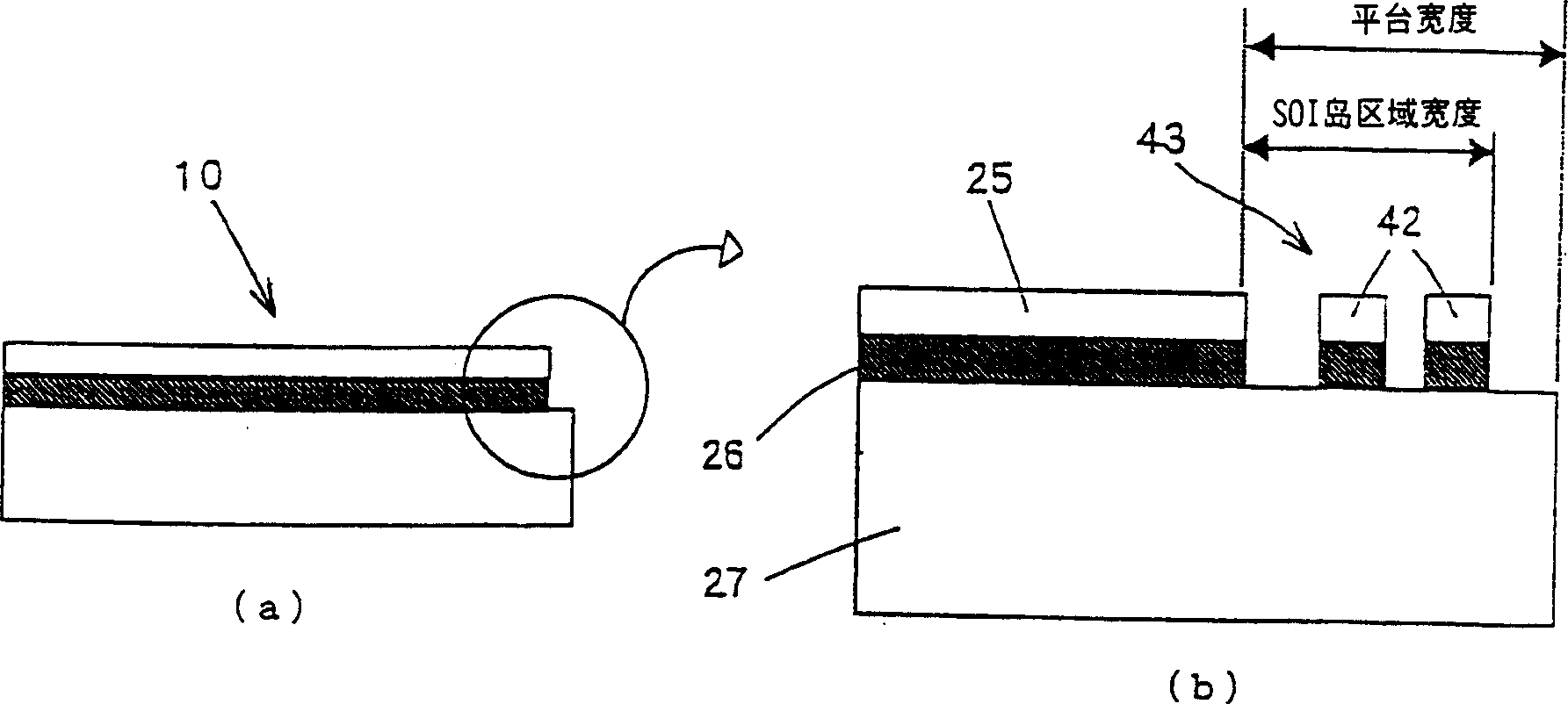
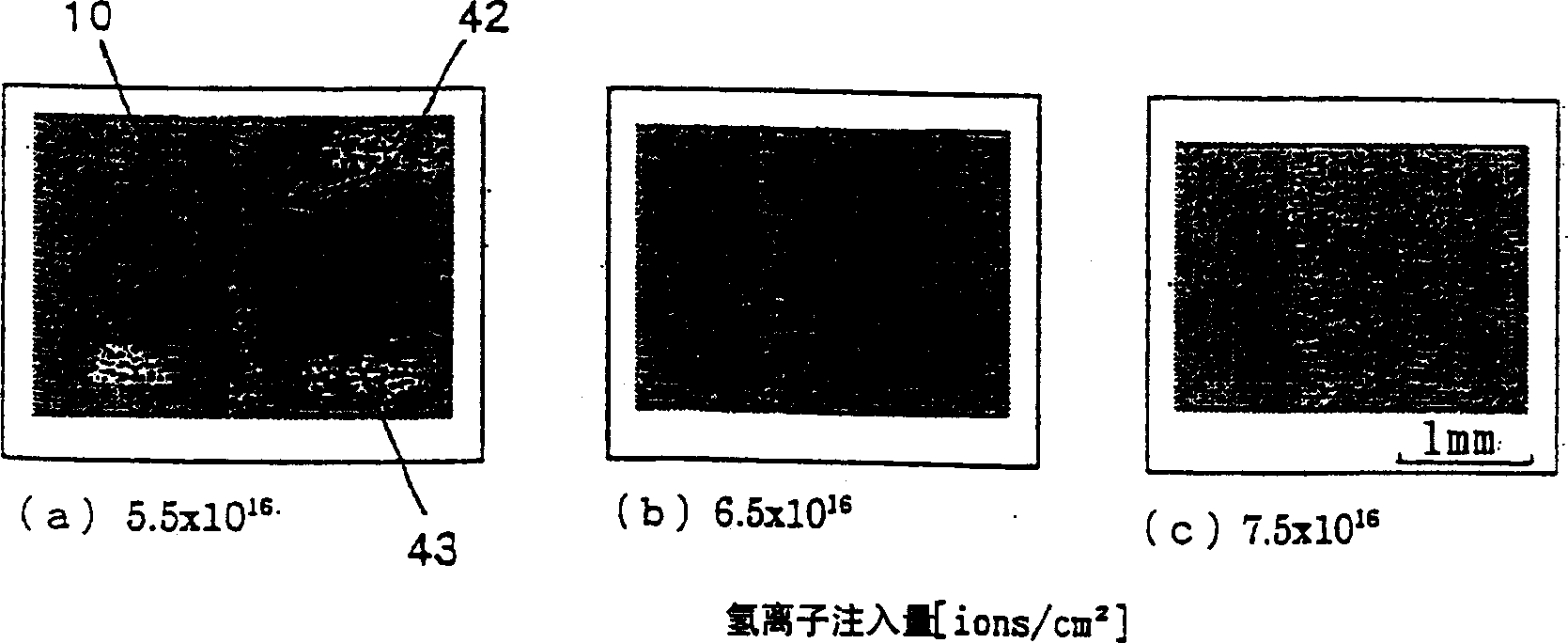
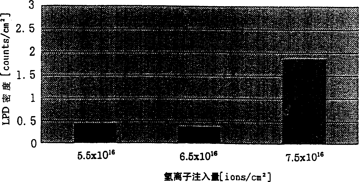
Abstract
Description
Claims
Application Information
 - R&D
- Intellectual Property
- Life Sciences
- Materials
- Tech Scout
- Unparalleled Data Quality
- Higher Quality Content
- 60% Fewer Hallucinations
Browse by: Latest US Patents, China's latest patents, Technical Efficacy Thesaurus, Application Domain, Technology Topic, Popular Technical Reports.
© 2025 PatSnap. All rights reserved.Legal|Privacy policy|Modern Slavery Act Transparency Statement|Sitemap|About US| Contact US: help@patsnap.com