Multi-layer distribution board and mfg method, electronic device and electronic apparatus

A technology of multilayer circuit board and manufacturing method, which is applied in the direction of multilayer circuit manufacturing, printed circuit manufacturing, electric solid-state devices, etc., and can solve problems such as disconnection of wiring layers, reduced use efficiency, and unevenness of the upper layer of the inner insulating film. Achieve the effects of avoiding open circuit, uniform film thickness and excellent insulation performance

Inactive Publication Date: 2004-06-09
SEIKO EPSON CORP
View PDF2 Cites 21 Cited by
  • Summary
  • Abstract
  • Description
  • Claims
  • Application Information

AI Technical Summary

Problems solved by technology

Then, in the wiring layer, the inner layer insulating film is formed in conformity with the uneven circuit pattern, and the flatness of the inner layer insulating film is insufficient.
With such an uneven interlayer insulating film, the upper part of the interlayer insulating film is also uneven, so that a flat wiring layer cannot be formed.
In addition, the cross-sectional shape of the upper inner layer insulating film or wiring layer will also be affected, resulting in disconnection between the wiring layers.
If the substrate is rotated, the material usage efficiency will be reduced and additional processes such as cleaning the backside will be required

Method used


Image

  • Multi-layer distribution board and mfg method, electronic device and electronic apparatus
  • Multi-layer distribution board and mfg method, electronic device and electronic apparatus
  • Multi-layer distribution board and mfg method, electronic device and electronic apparatus

Examples


no. 1 example

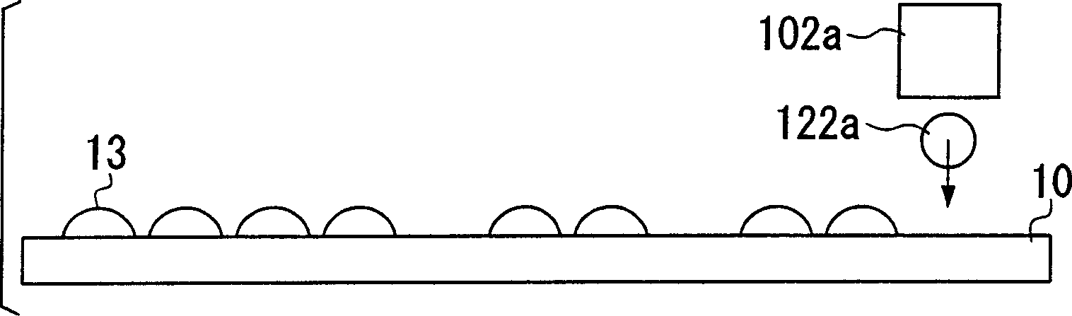
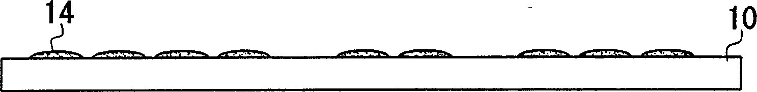
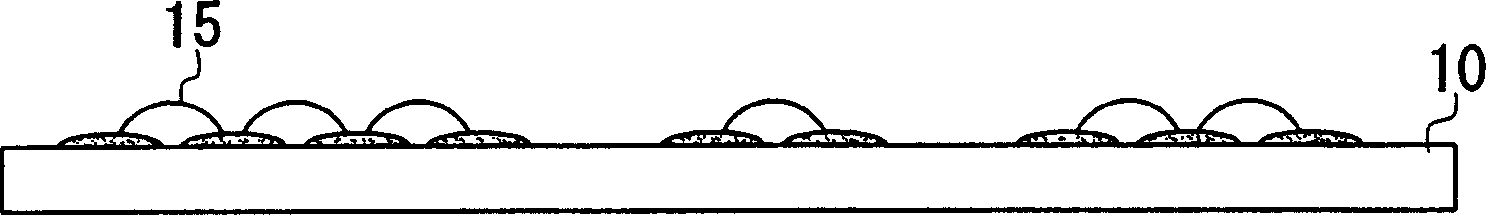
[0077] Figures 1A-3C It is a schematic diagram showing each process of the multilayer circuit board manufacturing method according to the first embodiment of the present invention. Figures 1A-1H Represents various processes from the ink repellent coating process to the process of forming the first circuit pattern (ie, the first wiring layer) and the inner layer conductive pillars. Figure 2A -2H indicates the process of forming the first interlayer insulating film. Figures 3A-3C Indicates that a second circuit pattern (ie, a second wiring layer) is formed. The respective processes of the second interlayer insulating film and the third circuit pattern (ie, the third wiring layer). In the present embodiment, multilayer printed wiring is formed on one surface of the substrate 10 .

[0078] Figure 4A with 4B is a schematic diagram showing a droplet ejection apparatus used in a method of fabricating a multilayer circuit board. Figure 4A is a perspective view showing the g...

no. 2 example

[0143] Image 6 is a schematic diagram showing a step in the method for manufacturing a multilayer circuit board according to the second embodiment of the present invention. In this embodiment, instead of the calculation process of the insulating film formation area in the first embodiment, the measurement process of the insulating film formation area is carried out. Other processes are the same as those of the first embodiment.

[0144] Processes different from those of the first embodiment will be described in detail below. Regarding other processes, only a series of flows of the respective processes of forming a multilayer circuit board will be described. Image 6 in, with Figure 1A to Figure 4B The same parts are given the same reference numerals.

[0145] In the multilayer circuit board manufacturing method of the present embodiment, (i) the ink repelling process to the substrate 10, (ii) the first circuit pattern forming process, and (iii) the inner layer conductive...

no. 3 example

[0162] Figures 8A to 8E It is a schematic diagram showing each step in the method for manufacturing a multilayer circuit board according to the third embodiment of the present invention. In this embodiment, a plurality of inner-layer insulating films are formed, and after the first inner-layer insulating film is formed, each height difference in the upper surface of the first inner-layer insulating film is measured, and the second inner layer is formed according to the measured data. insulating film to make the upper surface of the first inner layer insulating film flat.

[0163] Only the processes different from those of the first and second embodiments will be described in detail below. Regarding other processes, only a series of flows of the respective processes of forming a multilayer circuit board will be described. Figures 8A to 8E , with Figure 1 to Figure 7 The same parts are given the same reference numerals.

[0164] In the multilayer circuit board manufacturi...


PUM


Abstract

A multilayer circuit board and a manufacturing method for producing the board via simple manufacturing processes employing a droplet jetting method, where the inter-layer insulating film can be easily made flat. The multilayer circuit board includes at least two wiring layers, an inter-layer insulating film provided between every adjacent two of the wiring layers, and conductive posts for providing electrical conductivity between the wiring layers. The manufacturing method includes the step of forming the inter-layer insulating film by changing the film thickness of the inter-layer insulating film according to a concavo-convex shape of an area where the inter-layer insulating film is formed, so as to level an upper surface of the inter-layer insulating film. The concavo-convex shape may be computed based on design data of a circuit pattern for forming the wiring layers and the conductive posts, or may be measured before the inter-layer insulating film is formed.

Description

[0001] This application claims priority from Japanese Patent Applications No. 2002-334915 filed on Nov. 19, 2002 and No. 2003-300143 filed on Aug. 25, 2003, the contents of which are incorporated herein by reference. technical field [0002] The invention relates to a multilayer circuit board, a manufacturing method, an electronic device and an electronic device. Background technique [0003] In general, inner layer insulating films used in multilayer printed circuit boards are generally produced by spin coating or roll coating. According to the spin coating method, after dropping a liquid material on the substrate, the substrate is rotated to coat the entire surface of the substrate with the liquid material to form an insulating film. In roll coating, the solvent film is transferred to a press roll. But in the spin coating method, the actual material usage efficiency is close to 10%, and additional processes such as cleaning the backside are required. The roll coating met...

Claims


Application Information

Patent Timeline
Patent Type & Authority Applications(China)
IPC IPC(8): B41J2/01H05K1/02H05K3/00H05K3/12H05K3/46
CPCH05K2203/013H05K2203/1476H05K1/0269H05K3/4647H05K3/0005H05K2201/09881H05K3/125H05K3/4664H01L2224/11H01L2924/12044H01L2924/00H05K3/46
Inventor 桜田和昭
Owner SEIKO EPSON CORP
Why Eureka
Try Eureka