

Data erasing method for non volatile semiconductor storage
A non-volatile storage, data erasing technology, applied in static memory, read-only memory, information storage, etc., can solve the problem of difficult to achieve stable and high-speed erasing work
- Summary
- Abstract
- Description
- Claims
- Application Information
AI Technical Summary
Problems solved by technology
Method used
Image

Examples
Embodiment 1
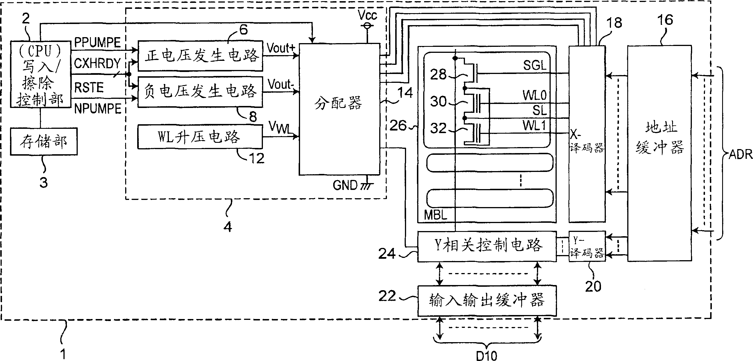
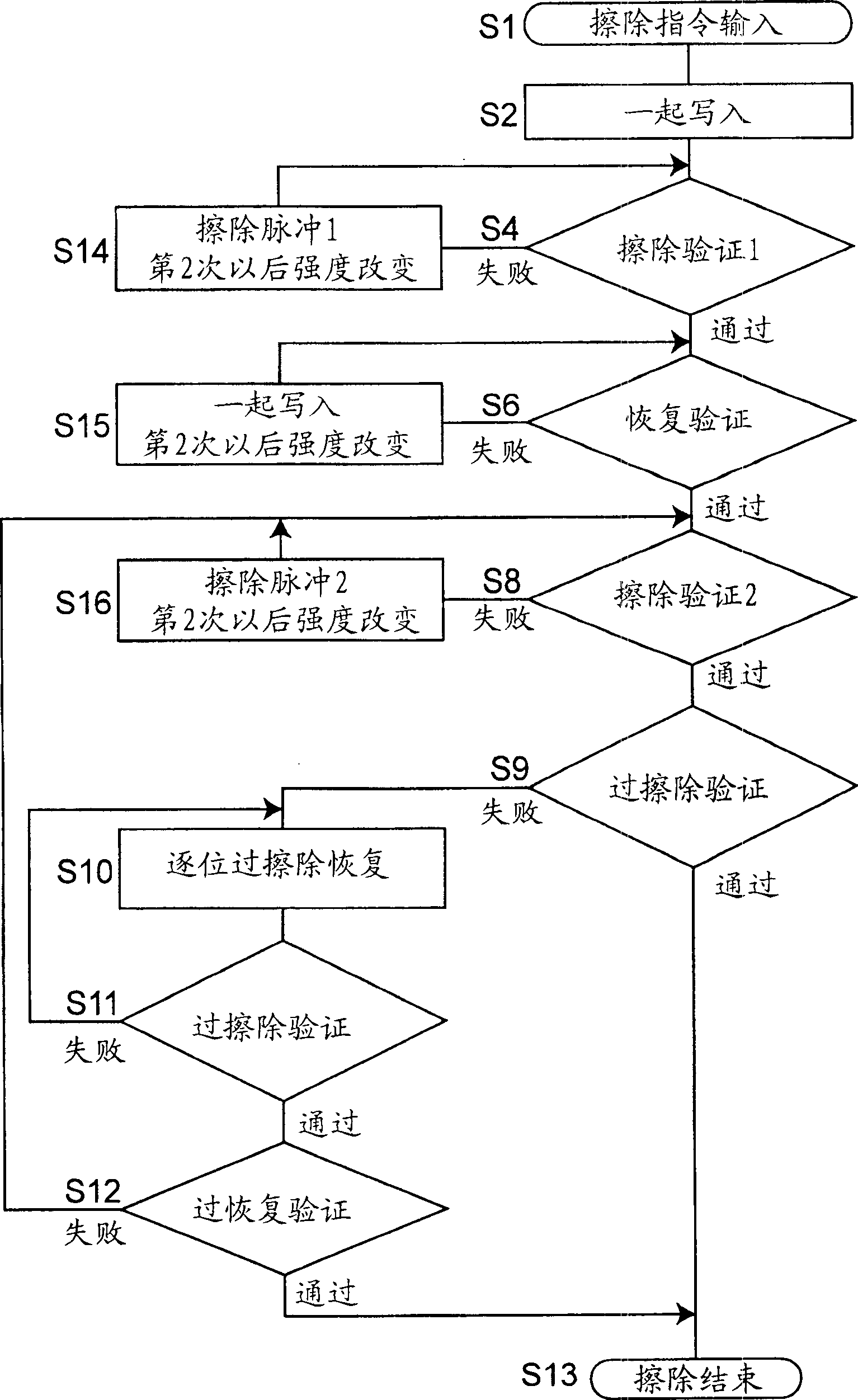
[0019] figure 1 It is a block diagram showing the schematic structure of the nonvolatile semiconductor memory 1 implementing the data erasing method of the present invention. This nonvolatile semiconductor memory 1 is formed of a flash memory using memory transistors as memory cells.
[0020] Like the conventional flash memory described above, this flash memory includes a plurality of nonvolatile memory transistors arranged in a matrix, a plurality of word lines for selecting rows of the memory transistors, and a plurality of word lines corresponding to the columns of the memory transistors respectively. A plurality of bit lines arranged in the ground are divided into a memory cell array of a plurality of memory blocks at the same time; a potential generating part that generates a potential applied to a word line, a bit line, a substrate part and a source of a memory transistor; and controlling the above-mentioned potential generating part , a write / erase control section that...
Embodiment 2
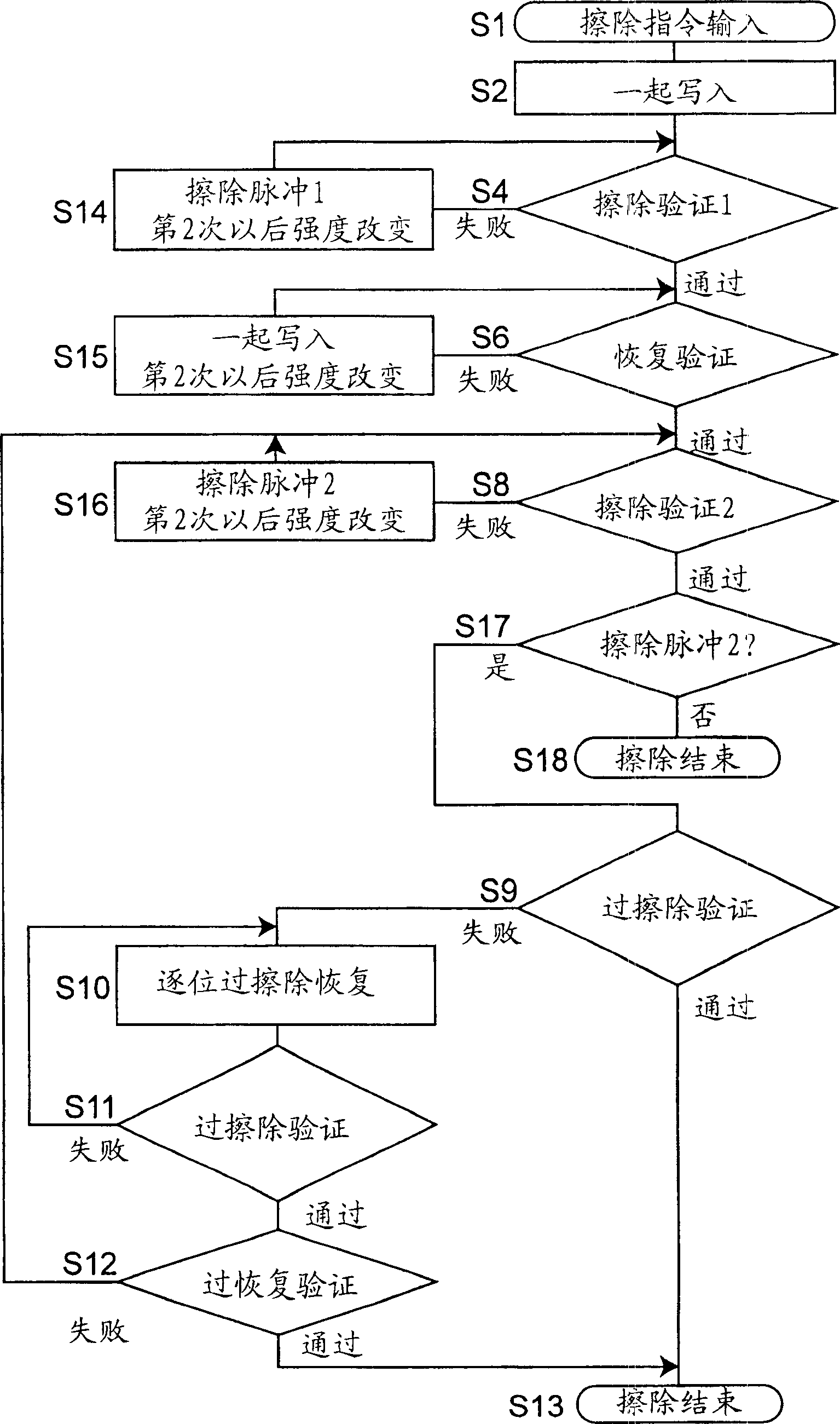
[0039] image 3 is a flowchart showing a data erasing method of the nonvolatile semiconductor memory 1 according to Embodiment 2 of the present invention. In contrast to Embodiment 1, in this embodiment, the erasure verification step S9 is performed only when the second erase pulse is applied, so that the erasing operation can be performed at a higher speed. For this purpose, in image 3 A step 17 of judging whether or not a second erase pulse is also applied to the memory transistor is added after the second erase verification step S8. When "No" in step S17, data erasing is ended in step S18. On the contrary, when step S17 is "Yes", the flow enters erasure verification step S9.
[0040] In this erasing work, by optimizing the conditions of step S14 of applying the first erasing pulse, step S15 of applying the programming pulse, step S16 of applying the second erasing pulse and recovery verification step S6, the The procedure of the over-erase verify operation and the over...
Embodiment 3
[0043] Figure 4 and Figure 5 is a flowchart showing a data erasing method of the nonvolatile semiconductor memory 1 according to Embodiment 3 of the present invention. In contrast to Embodiment 2, in this embodiment, in the second erasing verification step S8, a voltage of 0V is applied to the non-selected word lines, and at the same time, the over-erasing verification and over-erasing recovery steps S9-S12 are divided into the second There are two stages of steps S9 to S12 in the first stage and steps S19 to S22 in the second stage.
[0044] In this embodiment, since a voltage of 0V is applied to the non-selected word line in the second erasing verification step S8, the over-erasing verification and over-erasing recovery steps S9-S12 are also divided into the first stage steps S9-S12 and the second stage of steps S19 to S22, so it is possible to prevent the occurrence of read errors after the erasing is completed.
PUM
 Abstract
Description
Claims
Application Information