Pixel arrangement of active matrix form display
An active matrix and pixel structure technology, applied in the field of pixel structure, can solve the problems of labor and time consumption, uneconomical, inability to effectively repair 10 dead pixels of organic light-emitting displays, etc., so as to save processing time and improve product yield. Effect
- Summary
- Abstract
- Description
- Claims
- Application Information
AI Technical Summary
Problems solved by technology
Method used
Image

Examples
Embodiment Construction
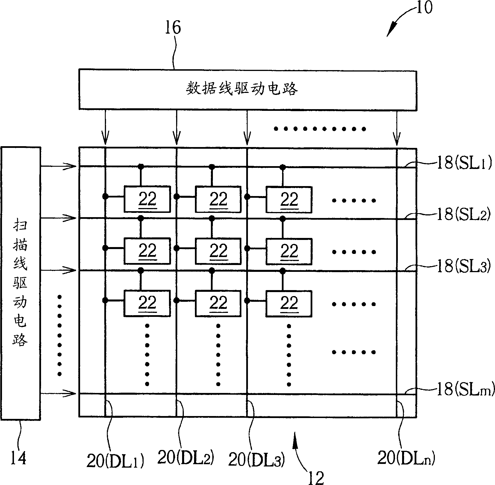
[0045] Please refer to Figure 5 , Figure 5 is a schematic diagram of the active matrix display 40 of the present invention. The active matrix display 40 includes a display panel 42 , a scan line driving circuit 44 and a data line driving circuit 46 . Wherein, the display panel 42 is provided with a plurality of scanning lines 48 (namely: SL 1 ~SL m ), a plurality of data lines 50 perpendicular to the scan lines 48 (ie: DL 1 ~DL n ), and a plurality of pixels 52 coupled to the scan line 48 and the data line 50. Generally speaking, the scan line driving circuit 44 and the data line driving circuit 46 input signals to the scan line 48 and the data line 50 respectively, so that each pixel 52 can present different gray levels according to the image data to form an image.
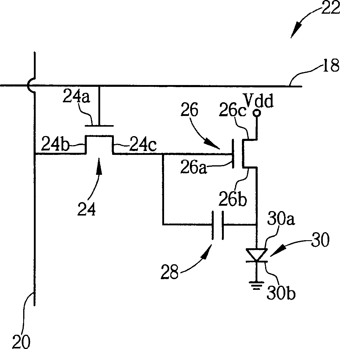
[0046] Please refer to Image 6 , Image 6 Yes Figure 5 A schematic circuit diagram of pixel 52 is shown. like Image 6 As shown, the pixel 52 includes a storage capacitor 54 , an active device 56 ,...
PUM
 Abstract
Description
Claims
Application Information
 - R&D
- Intellectual Property
- Life Sciences
- Materials
- Tech Scout
- Unparalleled Data Quality
- Higher Quality Content
- 60% Fewer Hallucinations
Browse by: Latest US Patents, China's latest patents, Technical Efficacy Thesaurus, Application Domain, Technology Topic, Popular Technical Reports.
© 2025 PatSnap. All rights reserved.Legal|Privacy policy|Modern Slavery Act Transparency Statement|Sitemap|About US| Contact US: help@patsnap.com