Upper electrode and plasma processing device

A plasma and electrode technology, applied in the direction of plasma, circuit, discharge tube, etc., can solve the problems of poor thermal conductivity and difficult temperature control

Active Publication Date: 2004-12-01
TOKYO ELECTRON LTD
View PDF2 Cites 17 Cited by
  • Summary
  • Abstract
  • Description
  • Claims
  • Application Information

AI Technical Summary

Problems solved by technology

[0012] However, such a structure that can be freely attached and detached has poor thermal conductivity, and it is difficult to perform high-precision temperature control

Method used


Image

  • Upper electrode and plasma processing device
  • Upper electrode and plasma processing device
  • Upper electrode and plasma processing device

Examples


Embodiment Construction

[0029] Hereinafter, embodiments of the present invention will be described in detail with reference to the accompanying drawings;

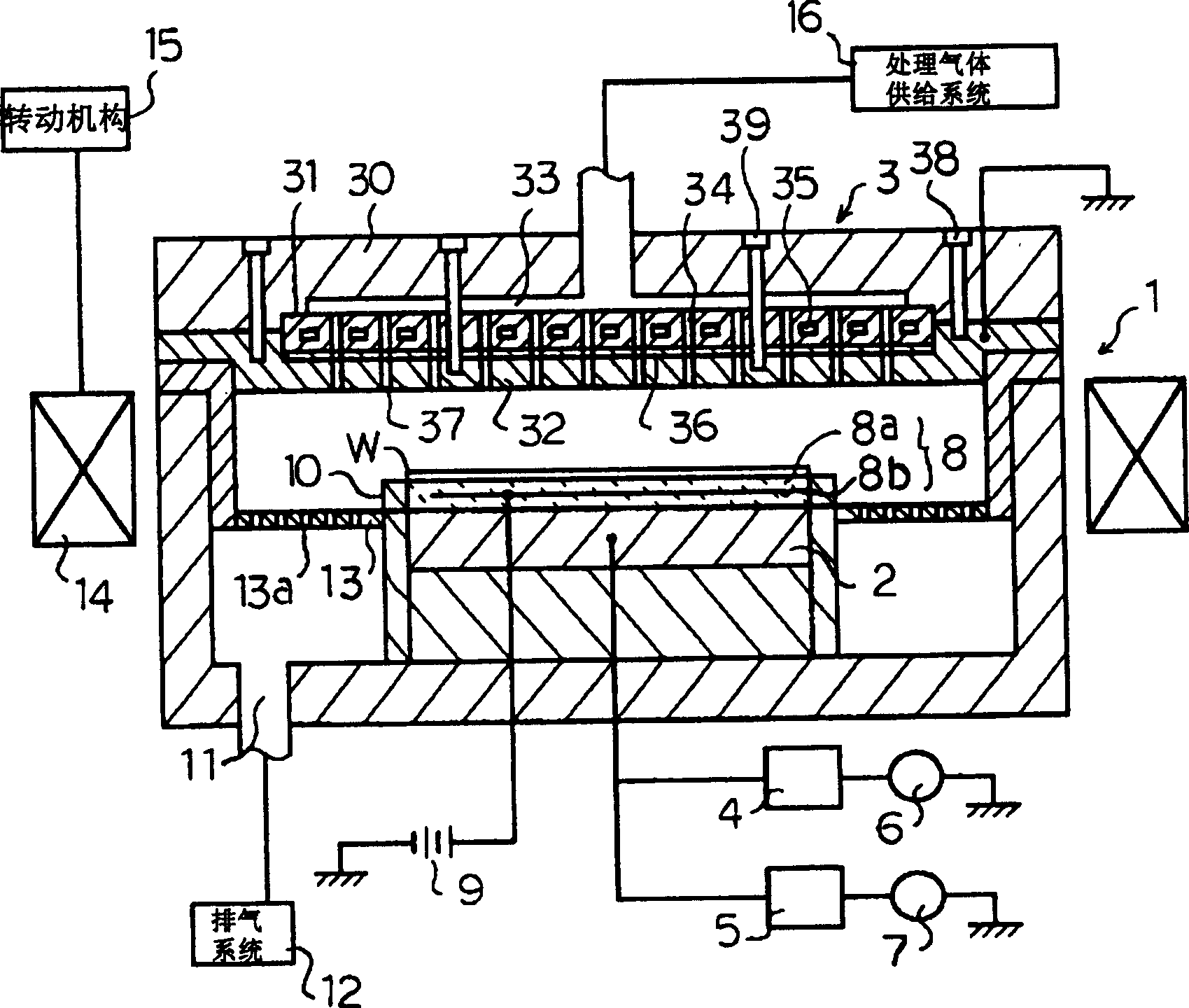
[0030] figure 1 A schematic configuration of an embodiment of the present invention applied to a plasma etching apparatus for etching a semiconductor wafer is schematically shown. In this figure, reference numeral 1 denotes a cylindrical vacuum chamber made of a material such as aluminum and having a hermetically sealed interior.

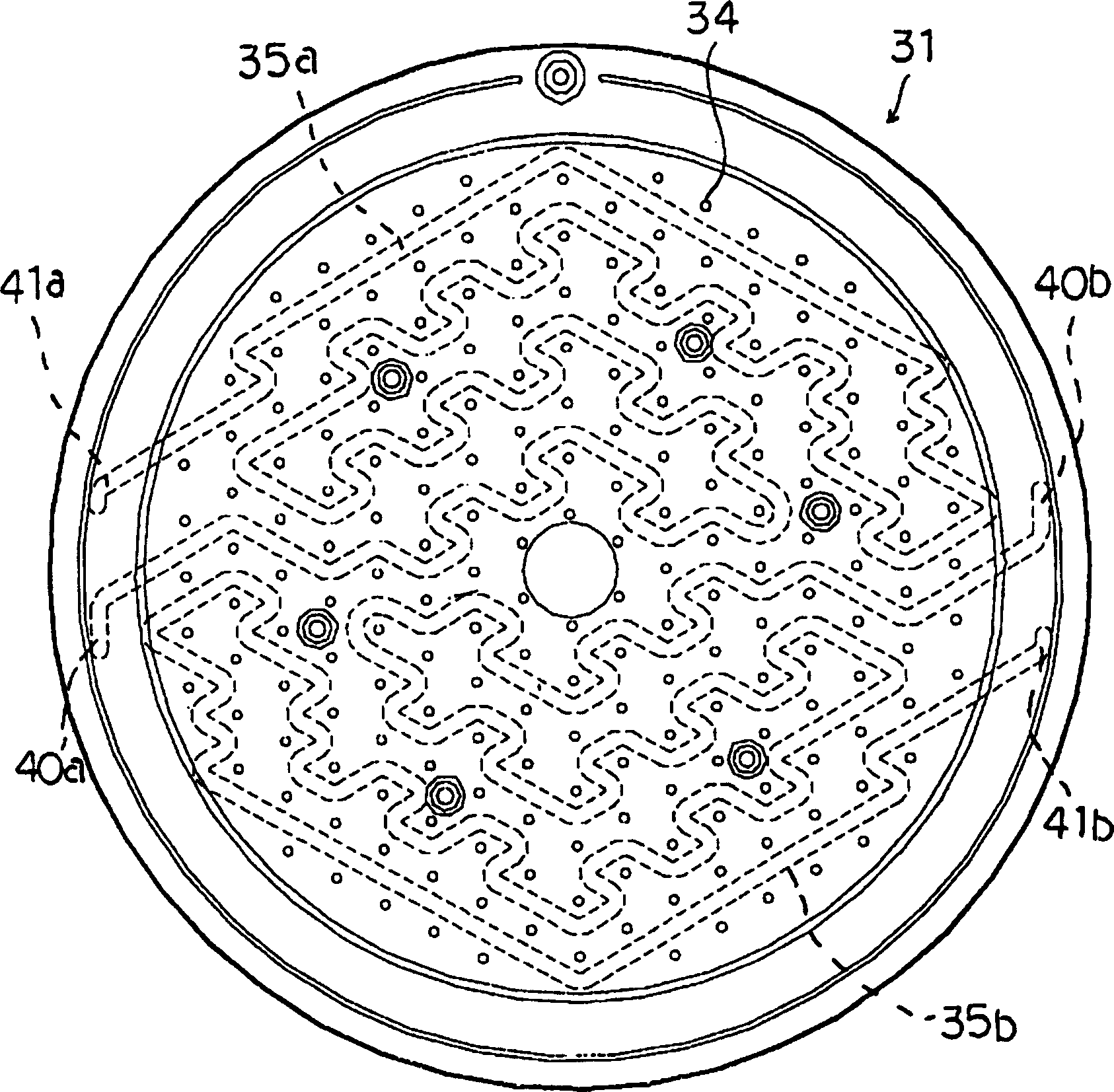
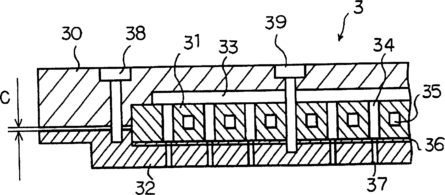
[0031] In this vacuum chamber 1, a stage 2 on which a semiconductor wafer W is placed is provided, and this stage 2 also serves as a lower electrode. In addition, on the top of the vacuum chamber 1, an upper electrode 3 constituting a shower head is provided. A pair of parallel plate electrodes is formed by the mounting table (lower electrode) 2 and the upper electrode 3 . The structure of the upper electrode 3 will be described in detail later.

[0032] Two high-frequency power sources 6, 7 are connected to the mou...


PUM


Abstract

Provided is an upper electrode which can be improved more in temperature controllability as compared with the conventional one while the running cost is reduced by suppressing the rise of the cost of a replaceable component and with which highly accurate plasma treatment can be performed, and to provide a plasma treatment device. The upper electrode 3 provided in a vacuum chamber 1 is constituted of a main electrode body 30, a cooling block 31, and an electrode plate 32. A process gas diffusing gap 33 is formed between the main electrode body 30 and the cooling block 31. In the cooling block 31, many through holes 34 are formed and finely bent refrigerant flow passages 35 are formed among the through holes 34. The electrode plate 32 is attachably / detachably fixed to the bottom side of the cooling block 31 through a flexible silicon rubber sheet 36 which is a heat transferring member, and discharge ports 37 are formed in the plate 32 correspondingly to the through holes 34.

Description

technical field [0001] The present invention relates to an upper electrode and a plasma processing apparatus for performing predetermined plasma processing such as etching processing or film forming processing by applying plasma to a substrate to be processed, such as a semiconductor wafer or a glass substrate for a liquid crystal display device. Background technique [0002] Previously, in the field of manufacturing semiconductor devices, plasma was generated in a vacuum chamber, and the plasma was applied to a substrate to be processed, such as a semiconductor wafer or a glass substrate for a liquid crystal display device, to perform predetermined processing such as etching or forming. Plasma processing equipment for film processing, etc. [0003] Such a plasma processing apparatus is a so-called parallel plate type plasma processing apparatus. A stage (lower electrode) on which a semiconductor wafer or the like is placed is provided in the vacuum chamber. At the same ti...

Claims


Application Information

Patent Timeline
Patent Type & Authority Applications(China)
IPC IPC(8): H05H1/46B01J3/00B01J19/08C23C16/44C23C16/455C23C16/509C23F4/00H01J37/32H01L21/02H01L21/3065
CPCC23C16/45565H01J37/3244H01J37/32724H01J37/32009C23C16/5096H01L21/02
Inventor 林大辅石田寿文木村滋利
Owner TOKYO ELECTRON LTD
Why Eureka
Try Eureka