

Printing preparation of mini gap reversed-mounting welded convex templates with lead/tin or leadless solder
A template and technology technology, which is applied in the field of preparing flip-chip bump solder balls, can solve the problems of poor reliability, affecting the life of solder balls, process limitations, etc., and achieve the effect of reducing solder ball spacing and improving process controllability
- Summary
- Abstract
- Description
- Claims
- Application Information
AI Technical Summary
Problems solved by technology
Method used
Image

Examples
Embodiment Construction
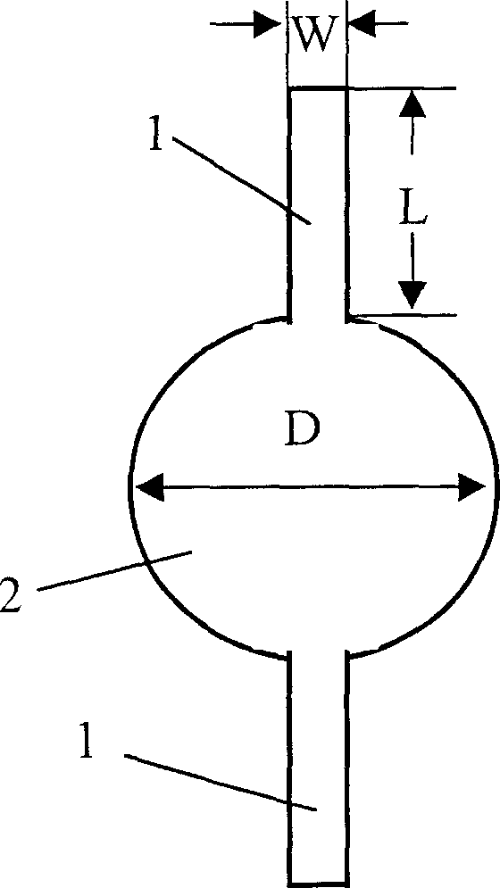
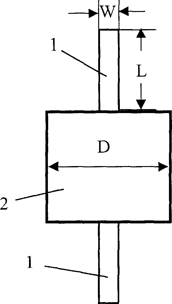
[0033] The UBM layer 2 to be prepared, such as figure 1 Shown as round or figure 2 is a square. Wherein, a pair of rectangular metal layers formed in two opposite directions of the UBM layer 2 is called the solder reflow guide layer 1 . The width W of the rectangular solder reflow guide layer 1 and the side length of the square ( figure 2 ) or circle diameter D( figure 1 ) ratio is between 0.08-0.15, and the ratio between the length L of the rectangular solder reflow guiding layer 1 and the side length or circle diameter D of a regular square is between 0-1.2.
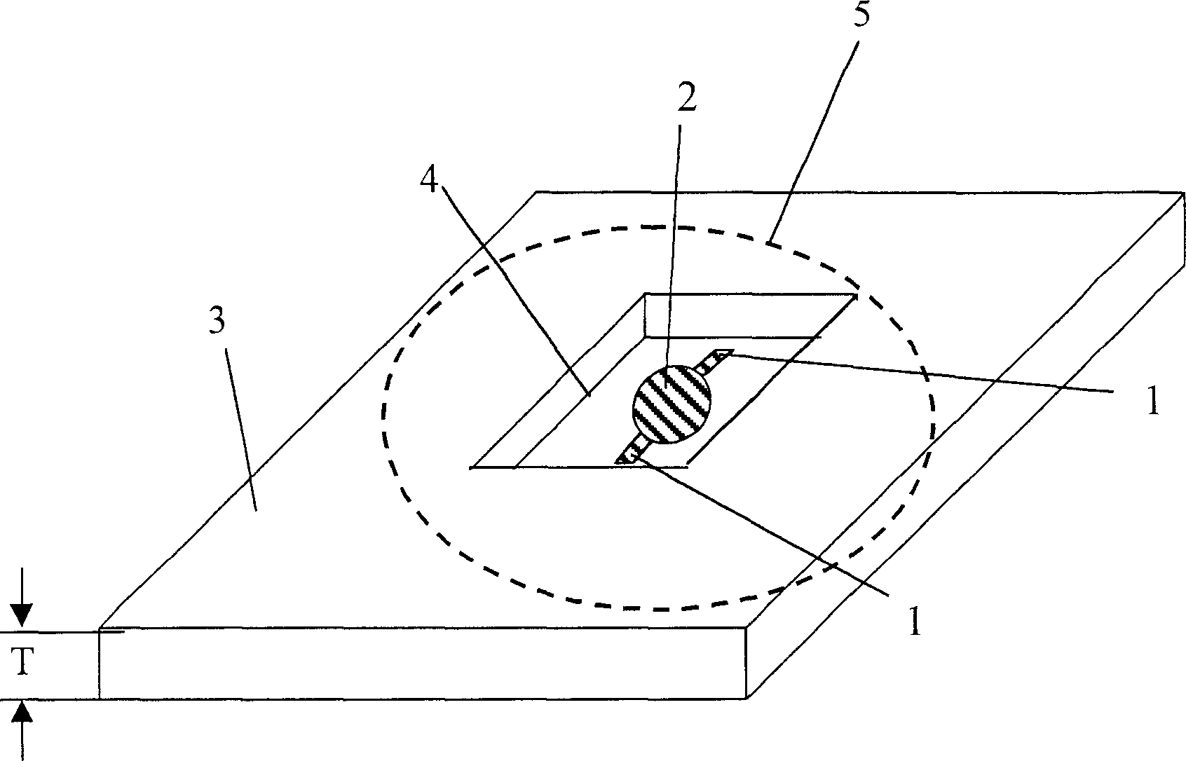
[0034] Such as image 3 As shown, that is, the printing template 3 used in FIG. 8( a ) is designed in such a way that the size of the template opening 4 needs to match the size of the UBM layer 2 and the reflow guide layer 1 .
[0035] As shown in Figure 4, the volume of 4 holes (V2) at the opening of the template is related to the thickness T of the template and the area of the opening, and the ratio of the v...
PUM
 Abstract
Description
Claims
Application Information