Synchronous single nort SRAM capable of realizng synchronous double port SRAM effect and its realizing method
An implementation method and a technology of corresponding functions, which are applied in the field of synchronous single-port SRAM and its implementation, can solve problems such as increased chip costs, and achieve the effect of reducing the volume
- Summary
- Abstract
- Description
- Claims
- Application Information
AI Technical Summary
Problems solved by technology
Method used
Image
Examples
Embodiment Construction
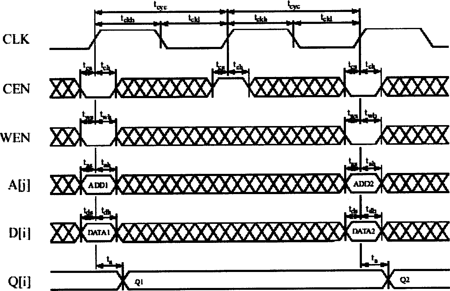
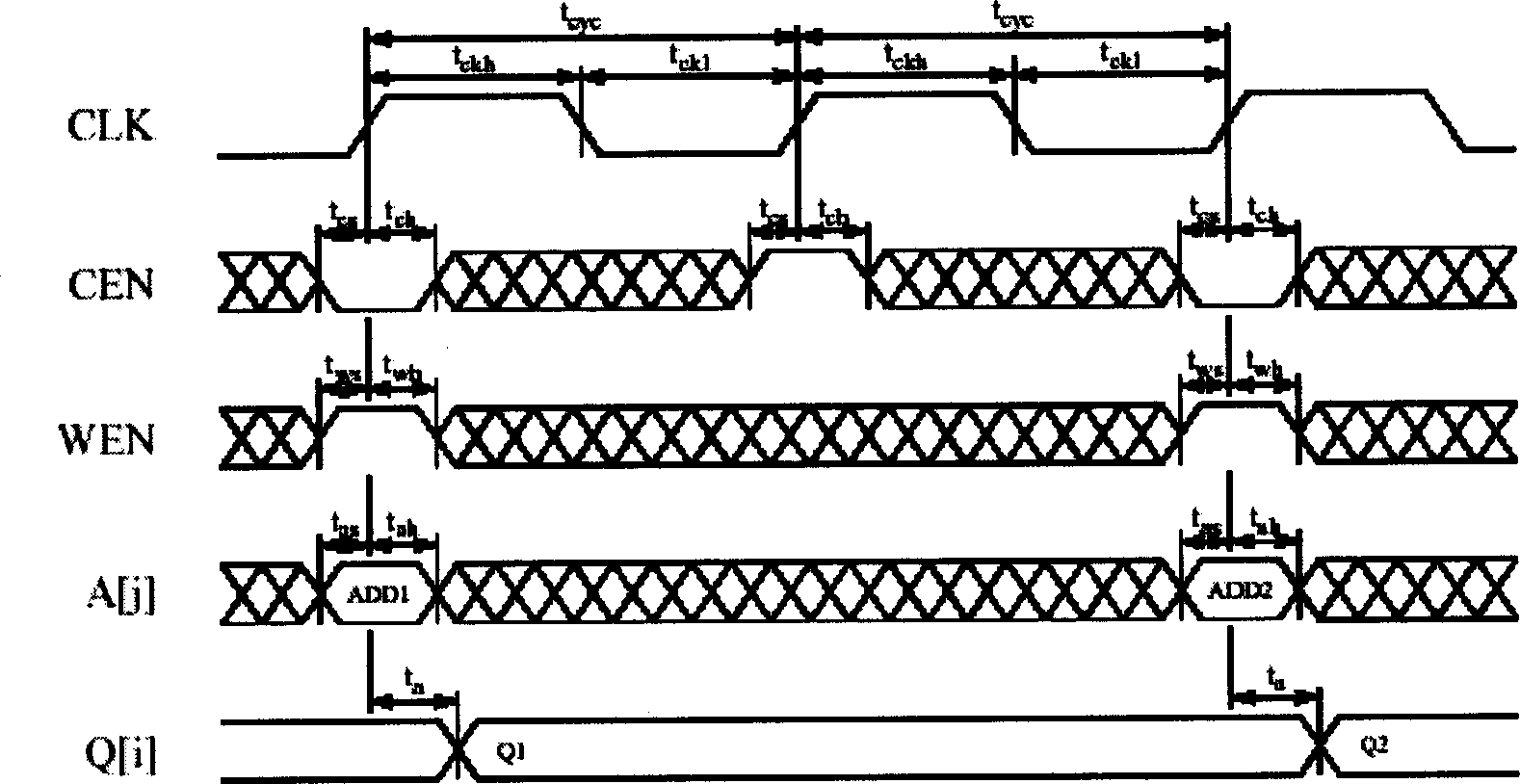
[0019] Refer to attached figure 1 , 2 , is a synchronous single-port SRAM write and read timing diagram.
[0020] The port signals of synchronous single-port SRAM generally include data input terminal D, data output terminal Q, address ADDR, clock CLK, block enable terminal CEN, write enable terminal WEN, and read enable terminal OEN; the port signals of synchronous dual-port SRAM are: Two such sets of signals: DA, DB, QA, QB, AA, AB, CLKA, CLKB, CENA, CENB, WENA, WENB, OENA, OENB. Sometimes write enable and read enable use a line WEN / OE, where tcyc is the clock cycle, tckl is the low time of the clock, tckh is the high time of the clock, tas is the address establishment time, and tah is the address Hold time, tds is the input data setup time, tdh is the address input data hold time, tws is the write signal setup time, twh is the write signal hold time, tcs is the block enable signal setup time, tch is the block enable signal hold time, When writing synchronous single-port ...
PUM
 Abstract
Description
Claims
Application Information
 - R&D
- Intellectual Property
- Life Sciences
- Materials
- Tech Scout
- Unparalleled Data Quality
- Higher Quality Content
- 60% Fewer Hallucinations
Browse by: Latest US Patents, China's latest patents, Technical Efficacy Thesaurus, Application Domain, Technology Topic, Popular Technical Reports.
© 2025 PatSnap. All rights reserved.Legal|Privacy policy|Modern Slavery Act Transparency Statement|Sitemap|About US| Contact US: help@patsnap.com


