Wiring circuit board, manufacturing method for the wiring circuit board, and circuit module

A technology of wiring circuit substrate and manufacturing method, which is applied in the directions of printed circuit manufacturing, multilayer circuit manufacturing, removing conductive materials by chemical/electrolytic methods, etc., can solve the problems of time-consuming, low production efficiency of wiring circuit substrates, etc.

Inactive Publication Date: 2005-01-26
INVENSAS CORP
View PDF0 Cites 11 Cited by
  • Summary
  • Abstract
  • Description
  • Claims
  • Application Information

AI Technical Summary

Problems solved by technology

Therefore, a device for hot pressing is required, and since it takes time to perform hot pressing, there is a problem that the production efficiency of the printed circuit board is low.

Method used


Image

  • Wiring circuit board, manufacturing method for the wiring circuit board, and circuit module
  • Wiring circuit board, manufacturing method for the wiring circuit board, and circuit module
  • Wiring circuit board, manufacturing method for the wiring circuit board, and circuit module

Examples


Embodiment 1

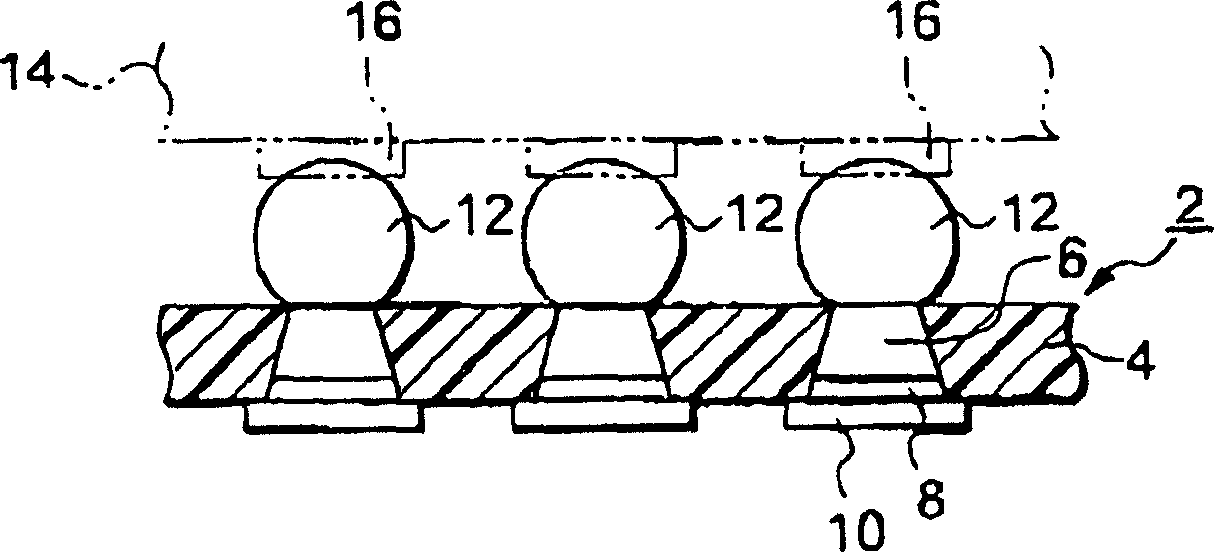
[0129] like figure 1 As shown, the wired circuit board 2 related to the first embodiment is composed of an insulating film 4 , a bump 6 , an etching stopper layer 8 , and a wiring layer 10 . The insulating film 4 is made of polyimide resin. The bump 6 is made of copper and formed to penetrate the insulating film 4 . In addition, the protrusion 6 has a conical shape. In more detail, the cross-sectional shape of the protrusion 6 is circular, and the vertical cross-section is roughly trapezoidal. In addition, the trapezoidal shape of the longitudinal section of the projection 6 is convenient for explanation, and the hypotenuse may also be curved. In addition, the longitudinal cross-sectional shape may be substantially rectangular, and the shape of the protrusion 6 may be substantially cylindrical instead of substantially conical. Even in such a case, the hypotenuse may be curved. In addition, the top surface of each protrusion 6 is exposed from the insulating film 4 , and i...

Embodiment 2

[0154] Next, refer to Figure 4 A wired circuit board related to Embodiment 2 of the present invention will be described. Figure 4 It is a cross-sectional view showing a wired circuit board related to Example 2. The wired circuit board related to Embodiment 2 has the same figure 1 The wired circuit boards related to the first embodiment shown have almost the same configuration, but differ in that the top surfaces 6 a of the protrusions 6 are formed as concave spherical surfaces. Therefore, the solder ball 12 is formed on the concave spherical surface.

[0155] Thus, according to the wired circuit board 2' related to the second embodiment, since the top surface 6a of each protrusion 6 is formed on the concave spherical surface, the connection area between the top surface 6a and the solder ball 12 is increased. As a result, the connection strength can be increased, the reliability of the printed circuit board can be improved, and the lifetime can be increased.

[0156] In ...

Embodiment 3

[0161] Next, refer to Figure 6A ~ Figure 6E A method of manufacturing a wired circuit board according to Embodiment 3 of the present invention will be described. Figure 6A ~ Figure 6E This is a cross-sectional view of the board showing the method of manufacturing the wired circuit board according to the third embodiment in order of steps. The method of manufacturing the wired circuit board according to the third embodiment is a method in which a part of the method of manufacturing the wired circuit board according to the first embodiment is modified.

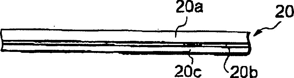
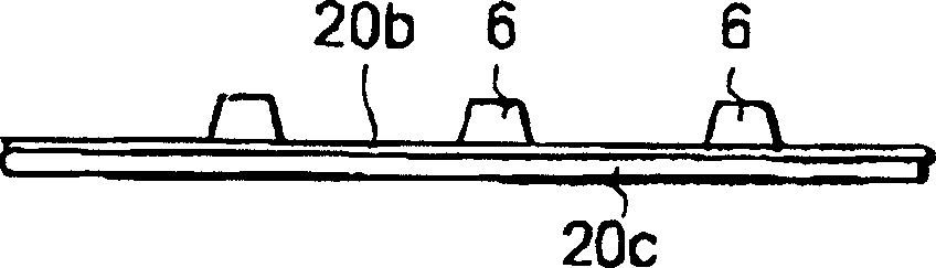
[0162] As shown in FIG. 6, the board|substrate 21 with a protrusion which formed the protrusion 6 on the one surface of the metal layer 20c for wiring layer formation via the etching stopper layer 20b is prepared. Through Example 1 Figure 2A ~ Figure 2C The procedure shown produces the substrate. Here, simply explain Figure 6A The fabrication method of the substrate is shown.

[0163] First, the multilayer metal plate 2...


PUM

PropertyMeasurementUnit
thicknessaaaaaaaaaa

Abstract

A manufacturing method for a wiring circuit board includes the steps of: forming a board on a surface of a metal layer directly or indirectly through an etching barrier layer; forming an insulating film on the surface of the metal layer; polishing the insulating film to an extent to which a top face of the bump is exposed; and forming a solder ball on the top face of the bump.

Description

technical field [0001] The present invention relates to a wiring circuit board for mounting electronic devices such as ICs and LSIs, for example. In particular, it relates to a wired circuit board capable of high-density mounting, a method for manufacturing the wired circuit board, and a circuit module including the wired circuit board. Background technique [0002] The progress of semiconductor manufacturing technology in recent years has been remarkable, and the miniaturization of semiconductor elements has been realized due to the rapid progress of fine pattern formation technology such as mask processing technology and etching technology. Therefore, in order to achieve high integration of the wiring board, it is necessary to multilayer the wiring board and to finely form connections between the upper and lower wiring films with high reliability. [0003] The applicant has developed a technique for manufacturing a multilayer wired circuit board by etching a metal film su...

Claims


Application Information

Patent Timeline
Patent Type & Authority Applications(China)
IPC IPC(8): H05K1/02H01L21/48H01L23/31H01L23/498H01L23/538H01L25/10H05K1/00H05K1/11H05K1/16H05K3/06H05K3/10H05K3/34H05K3/36H05K3/40H05K3/46
CPCH01L2924/01049H01L2225/1041H05K2201/0195H01L25/105H01L2224/73265H01L2924/01045H05K2203/0384H05K3/108H01L2224/16H05K3/3457H01L2224/48091H01L23/49816H01L2924/01078H01L23/5387H01L24/48H01L2924/14H05K3/4632H01L21/4857H01L2924/01041H05K1/0393H01L2924/01024H01L2924/12041H01L2224/45144H01L2924/01013H01L2924/15331H05K3/4617H05K3/4626H05K3/4652H05K2201/09509H05K1/113H01L2224/32225H01L2924/0105H05K3/06H05K3/4038H01L2924/01047H01L2224/16225H01L2924/01006H01L2924/3025H01L2924/19041H05K2203/1476H01L2924/01079H01L2924/01073H05K3/363H01L2924/15311H05K2201/0154H01L21/4853H01L2224/32145H01L2224/73204H01L2225/1023H01L2924/01082H05K2201/0129H05K2201/0355H05K3/4655H05K1/167H01L2924/01023H05K2203/0733H01L2224/48471H01L2924/07811H01L2924/01029H01L2225/1058H01L2924/19043H01L23/49822H01L24/32H01L2224/48227H05K3/062H01L2924/01033H01L23/3128H05K1/115H01L23/49827H05K2201/096H01L2224/16235H01L2924/00014H01L2924/12042H01L24/45H01L24/73H01L2924/181Y10T29/49124Y10T29/49213H01L2924/00H01L2924/00012H01L2224/05599H05K1/02
Inventor 饭岛朝雄远藤仁誉池永和夫大平洋三成尚人加藤贵
Owner INVENSAS CORP
Why Eureka
Try Eureka