Pixel position specifying method, method of correcting image offset, and image forming device

A technology of pixel position and specific method, which is applied in the direction of printing equipment, image communication, photolithography process exposure equipment, etc., can solve the problems of image quality reduction, difficulty in applying multi-head exposure equipment, etc., and achieve the effect of preventing offset or overlapping

Inactive Publication Date: 2005-02-02
FUJIFILM CORP
View PDF1 Cites 4 Cited by
  • Summary
  • Abstract
  • Description
  • Claims
  • Application Information

AI Technical Summary

Problems solved by technology

[0007] Furthermore, the problem with the exposure head is that due to the use of many optical components and mechanical components from the light source to the imaging surface, each component undergoes thermal expansion and thermal contraction as the temperature changes. For each image head of the above image, the offset or overlap generated at the connection point will reach a non-negligible level, resulting in a decrease in image quality
[0009] However, in a multi-head exposure device, the above method is difficult to apply to a multi-head exposure device because the distance between the exposure heads is much smaller than the distance between adjacent beams.

Method used


Image

  • Pixel position specifying method, method of correcting image offset, and image forming device
  • Pixel position specifying method, method of correcting image offset, and image forming device
  • Pixel position specifying method, method of correcting image offset, and image forming device

Examples


Embodiment approach 1

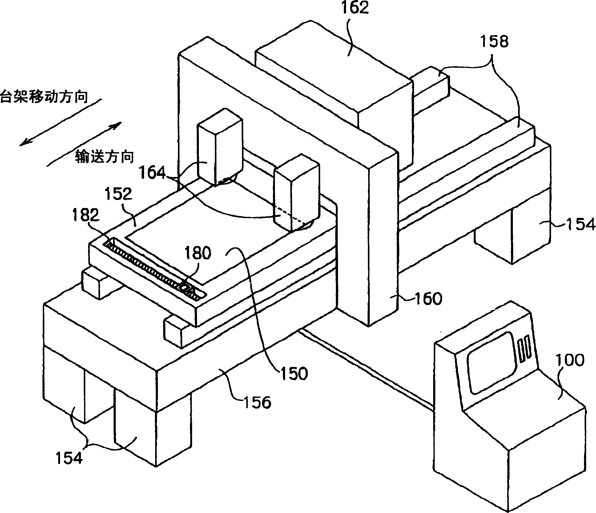
[0186] An example of the exposure device included in the image forming apparatus of the present invention, its overall configuration is shown in figure 1 .

[0187] The exposure apparatus of Embodiment 1 is a so-called flat plate type, such as figure 1 As shown, a stand 152 is provided which absorbs a sheet-shaped photosensitive material 150 on its surface to maintain a flat shape. The side surface of the stage 152 that absorbs and holds the photosensitive material 150 and the exposed surface of the photosensitive material 150 correspond to the image forming surface in the image forming apparatus of the present invention.

[0188] The above-mentioned exposure apparatus is equipped with a thick plate-shaped installation table 156 supported by four supports 154 and two guide rails 158 on the installation table 156 . Rail 158 is provided along the figure 1 The direction of gantry movement indicated by the arrow in the middle. The stage 152 is configured such that its longitud...

Embodiment approach 2

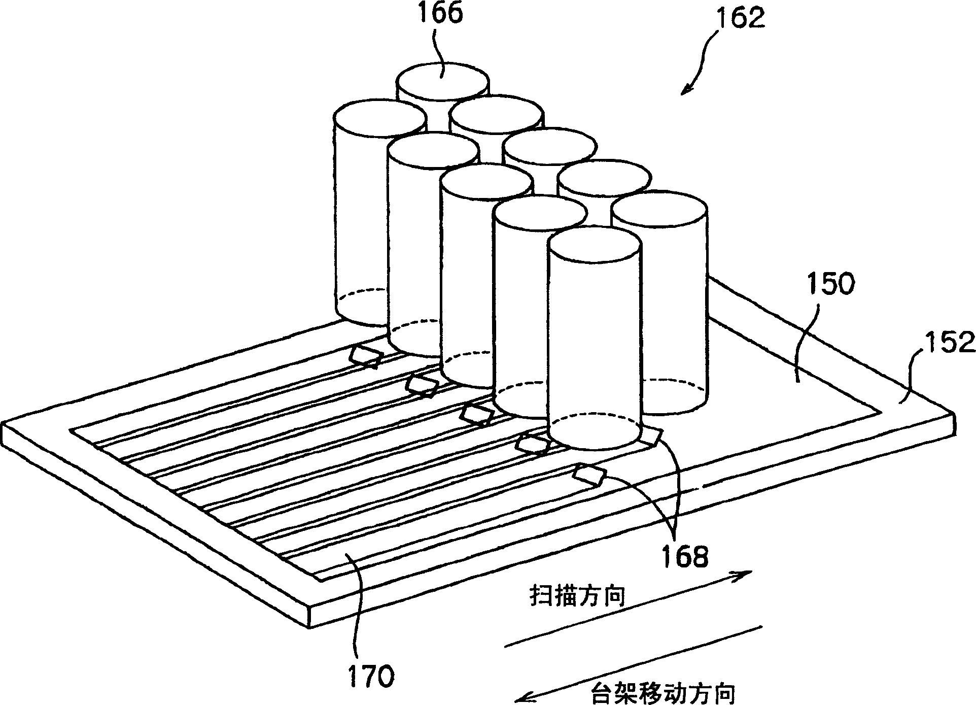
[0219] Regarding another example of the exposure device included in the image forming apparatus of the present invention, Figure 10 The overall configuration is shown in . For the same components as those in Embodiment 1, repeated explanations will be omitted. The same symbols as in Embodiment 1 denote the same constituent elements in principle.

[0220] Like the exposure apparatus of Embodiment 1, the exposure apparatus of Embodiment 2 is a so-called flat plate type, such as Figure 10 As shown, there is provided a plate-shaped stand 152 on which a sheet-shaped photosensitive material 150 is adsorbed and held on its surface.

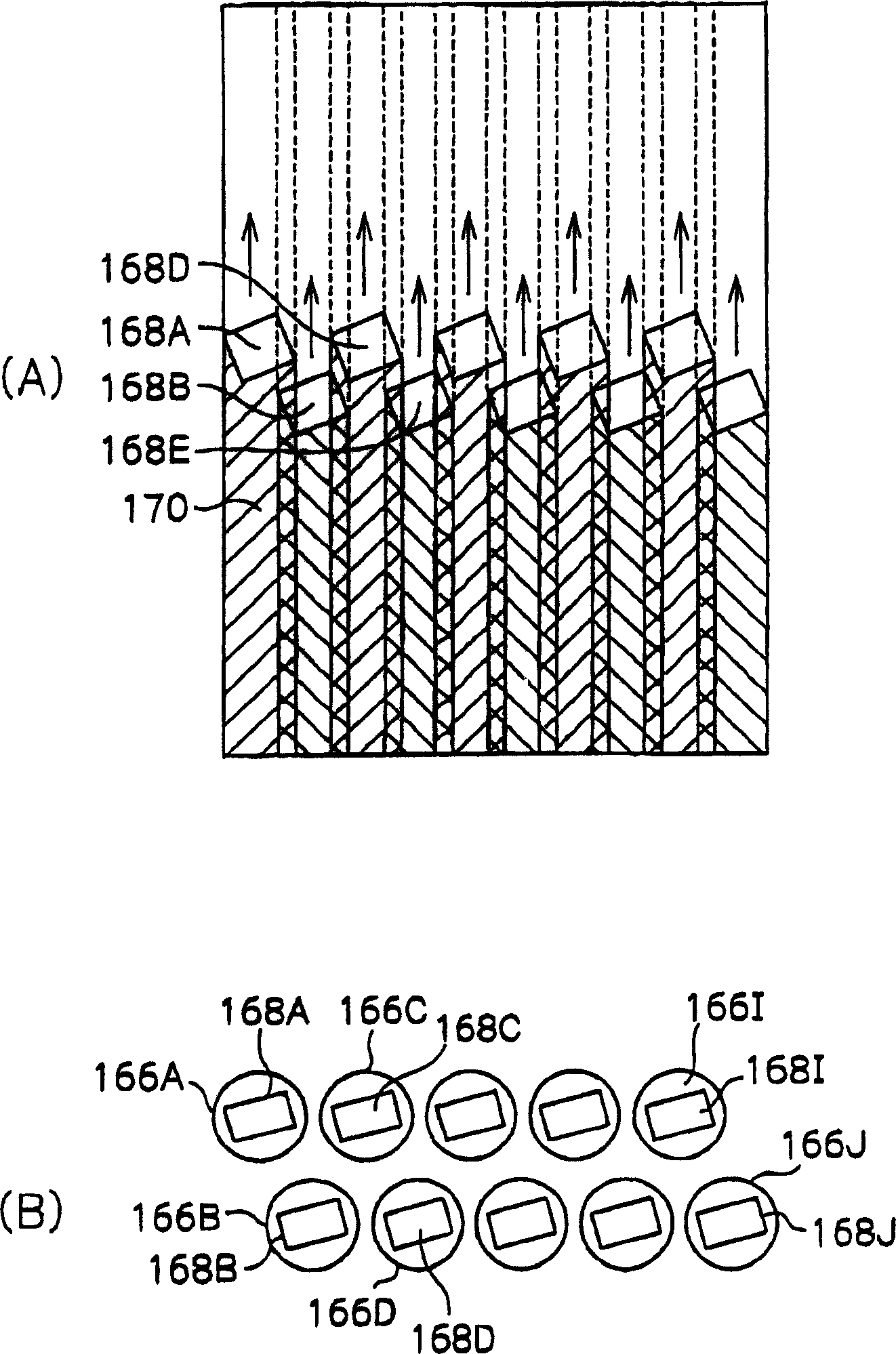
[0221]However, in the downstream end of the stage 152 along the stage moving direction, instead of the probe 180 included in the exposure apparatus according to Embodiment 1, a sensor is arranged along the X-axis direction, that is, in a direction perpendicular to the stage moving direction. A plane detector 184 with six plane detectors 184a-184f fi...

Embodiment approach 3

[0236] As another example of the exposure device included in the image forming apparatus of the present invention, its overall configuration is shown in Figure 12 middle. Descriptions of the same components as in Embodiment 1 are omitted, and the same symbols as in Embodiment 1 refer to the same components in principle.

[0237] The exposure apparatus of Embodiment 3 is the same as that of Embodiment 1, and is a so-called flat plate type, such as Figure 12 As shown, there is provided a plate-like stand 152 on which a sheet-like photosensitive material 150 is sucked and held on its surface.

[0238] However, at the end of the stage 152 on the downstream side in the stage moving direction, a surface probe 186 capable of moving in the X-axis direction by a high-precision transfer device 187 is provided, such as Figure 13 As shown, a groove 185 along the X-axis direction is provided over the entire width at the downstream end of the stand 152 . The face probe 186 slides in t...


PUM

PropertyMeasurementUnit
reflectanceaaaaaaaaaa

Abstract

The invention provides a pixel positioning method, an image shift correction method and an imaging device, which comprises following steps: opening a first connecting pixel near a connecting joint of a first exposure head; moving a beam position detector along a Y axis; detecting a first exposure beam position in XY coordinate on the light receiving side; opening a second connecting pixel near a connecting joint of a second exposure head; moving the beam position detector along the Y axis; detecting the exposure beam position in XY coordinate on the light receiving side; positioning the first pixel and second pixel according to the motion quantity of the beam position detector along the Y axis and the exposure beam positions of the first exposure head and the second exposure head on the light receiving side. The pixel positioning method and image shift correction method as well as the imaging device has the advantages of reducing shift among the images formed by the exposure heads in the multi-head exposure devices.

Description

technical field [0001] The present invention relates to a pixel position specifying method, an image offset correction method, and an image forming apparatus. In particular, in an image forming apparatus equipped with a plurality of exposure heads, even if the relative position between the exposure heads changes, the pixel position identification method can identify the positions of connected pixels in the exposure heads with high precision, and can form a connection point that is not conspicuous. An image shift correction method for a high-quality image, and an image forming apparatus for correcting image shift between exposure heads using the image shift correction method. Background technique [0002] Over the years, as an example of an image recording device, various exposure devices that use a spatial light modulation element (SLM) such as a digital micromirror device (DMD) to perform image exposure with a light beam modulated according to image data have been proposed....

Claims


Application Information

Patent Timeline
Patent Type & Authority Applications(China)
IPC IPC(8): B41J2/44B41J2/47G02B26/10G03B27/54G03F7/20H04N1/195H05G1/64
CPCG03F7/2051H04N1/19584G03F7/2053G03F7/70291H04N2201/0414H04N1/195G03F7/2055H04N1/1903G03F7/70466G03F7/20
Inventor 高田伦久
Owner FUJIFILM CORP
Why Eureka
Try Eureka