Method of manufacturing semiconductor device and manufacturing apparatus of semiconductor device

A manufacturing method and technology of a manufacturing device, which are applied in the fields of semiconductor/solid-state device manufacturing, semiconductor devices, electric solid-state devices, etc., can solve the problems of dull blade, increased incidence of defective semiconductor components, and easy access to component areas.

Inactive Publication Date: 2005-02-09
KK TOSHIBA
View PDF4 Cites 5 Cited by
  • Summary
  • Abstract
  • Description
  • Claims
  • Application Information

AI Technical Summary

Problems solved by technology

Therefore, the sticking film causes the edge of the cutting blade to be blocked, which makes the edge dull, which makes the back surface of the semiconductor element prone to large cracks.
Large cracks can be a bad cause of semiconductor elements
[0015] Especially in thinned semiconductor elements, not only the cracks on the back surface are easy to reach the element area, but also the cracks are easy to develop in the subsequent pick-up process and mounting process, which leads to an increase in the defect rate of semiconductor elements

Method used


Image

  • Method of manufacturing semiconductor device and manufacturing apparatus of semiconductor device
  • Method of manufacturing semiconductor device and manufacturing apparatus of semiconductor device
  • Method of manufacturing semiconductor device and manufacturing apparatus of semiconductor device

Examples


Embodiment Construction

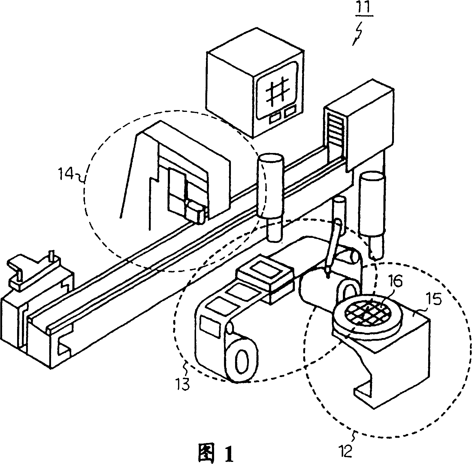
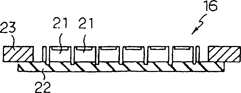
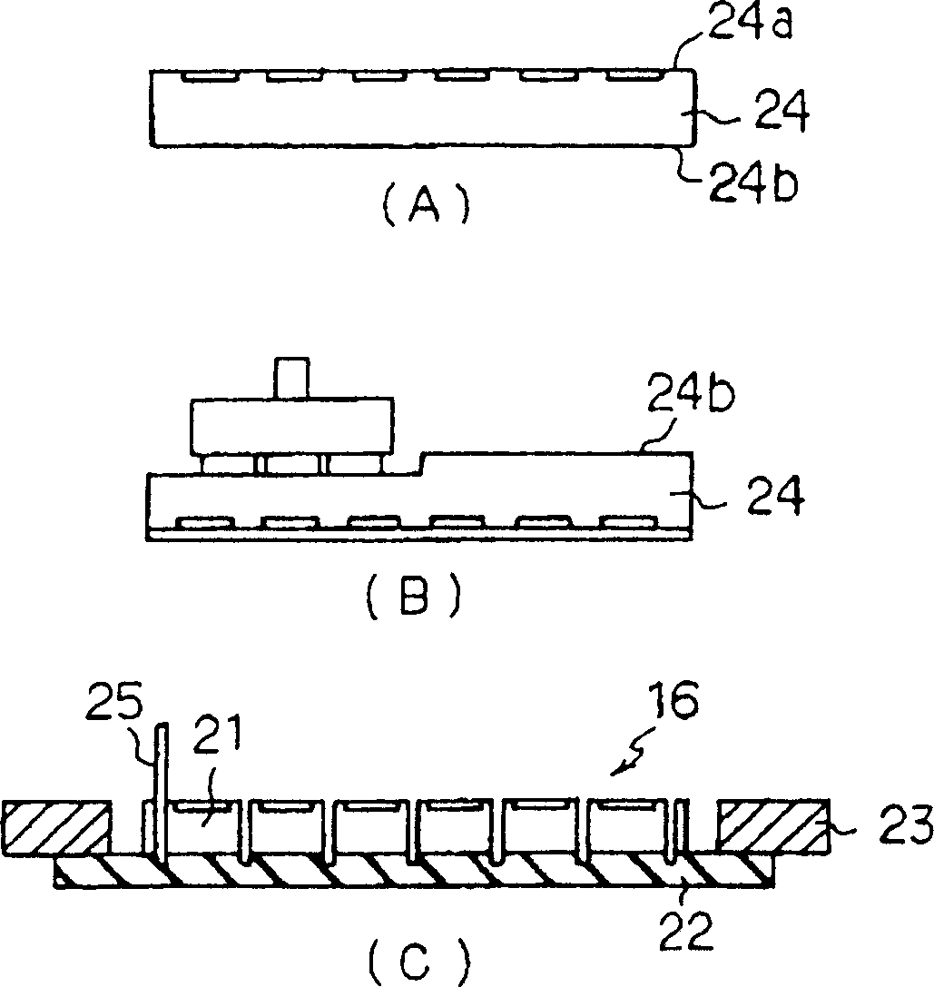
[0054] According to an embodiment of the manufacturing method of the semiconductor device and the semiconductor device of the present invention, first, the semiconductor wafer having the element region formed on the surface portion is cut and divided into individual small pieces of semiconductor elements. In this state, the semiconductor element is held by the holding member. Next, after the semiconductor element is picked up from the holding member for each element, the element bonding film which is separated into pieces according to the shape of the element is attached to the back surface of the semiconductor element. Thereafter, the semiconductor element is bonded to the base material for semiconductor device formation using the element bonding film attached to the back surface of the semiconductor element.

[0055] In one embodiment of the present invention, a holding tape such as an adhesive tape is used as the holding member. In addition, instead of the holding tape, a ...


PUM


Abstract

A manufacturing apparatus of a semiconductor device is provided with a pickup section for picking up a sectioned semiconductor element from a semiconductor wafer, a film sticking section for sticking an element adhesive film sectioned according to a shape of the element to the back surface of the semiconductor element, and an element adhesion section for adhering the semiconductor element to a semiconductor device forming base material. Chippings, which are caused when a thinned semiconductor wafer is diced, are suppressed so to reduce a failure incidence rate of the semiconductor device.

Description

technical field [0001] The present invention relates to a manufacturing method of a semiconductor device and a semiconductor manufacturing apparatus. Background technique [0002] The manufacturing process of a semiconductor device can be roughly divided into a process of forming various element patterns on the surface of a semiconductor wafer (semiconductor substrate), and a process of separating the semiconductor wafer into individual semiconductor elements and packaging the semiconductor elements with a package. In recent years, in order to reduce the manufacturing cost of semiconductor devices, the diameter of wafers has been increased. In addition, semiconductor wafers are being thinned in order to enable high-density mounting of semiconductor elements. [0003] A conventional semiconductor wafer slicing process will be described with reference to FIG. 18 . For example, as described in Patent Document 1 or Patent Document 2, a semiconductor wafer 1 having an element p...

Claims


Application Information

Patent Timeline
Patent Type & Authority Applications(China)
IPC IPC(8): H01L21/52H01L21/00H01L21/301H01L21/58H01L21/68
CPCH01L21/6836H01L2224/274H01L2224/83191H01L24/27H01L2924/01082H01L2221/68327H01L21/67132H01L2224/743H01L2224/48227H01L21/6835H01L24/83H01L24/743H01L24/29H01L2924/01005H01L2924/01033H01L2924/01006H01L2221/68322H01L2221/6834H01L2224/48091H01L2224/49171H01L2224/8385H01L2924/07802H01L2924/12042Y10T156/1075Y10T156/1179Y10T156/1978H01L2924/00014H01L2924/00H01L2924/3512
Inventor 黑泽哲也
Owner KK TOSHIBA
Why Eureka
Try Eureka