
Input buffer circuit, and semiconductor apparatus having the same

A technology of input buffer and buffer, applied in the direction of logic circuit, logic circuit connection/interface layout, logic circuit coupling/interface using field effect transistor, etc. The effect of misoperation and simplified circuit structure

Inactive Publication Date: 2005-02-09
SONY GRP CORP
View PDF1 Cites 1 Cited by
  • Summary
  • Abstract
  • Description
  • Claims
  • Application Information

AI Technical Summary

Problems solved by technology

If a malfunction of the external circuit occurs, there is a concern that various circuits connected to the input buffer circuit in the subsequent stage may not operate normally.

Method used


Image

  • Input buffer circuit, and semiconductor apparatus having the same
  • Input buffer circuit, and semiconductor apparatus having the same

Examples


Embodiment Construction

[0027] Specific embodiments of the present invention will be described below with reference to the accompanying drawings.

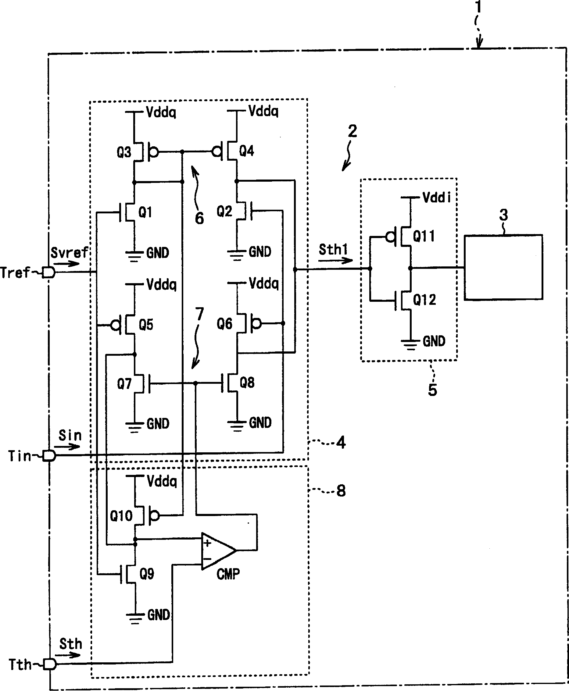
[0028] In the semiconductor device 1 according to the present invention, as figure 1 As shown, the internal processing circuit 3 is connected to the input buffer circuit 2.

[0029] The input buffer circuit 2 is composed of a first buffer circuit 4 on the input side and a second buffer circuit 5 on the output side, these first and second buffer circuits 4, 5 are driven by first The voltage Vddq and the second driving voltage Vddi are driven. Here, the first driving voltage Vddq is defined as an external power supply voltage used outside the semiconductor device. On the other hand, the second driving voltage Vddi is defined as an internal power supply voltage used inside the semiconductor device 1 .

[0030] The first buffer circuit 4 is composed of a pair of complementary (N-channel MOS input and P-channel MOS input) current mirror amplifiers 6 , 7 and...


PUM


Abstract

According to the present invention, an input buffer circuit comprises a first and a second buffer circuits operated at different first and second drive voltages and connected in turn, and an output potential control circuit is provided for carrying out a control so that, in spite of a voltage value of the first drive voltage, a threshold of an output potential of the first buffer circuit becomes a threshold of an input potential of the second buffer circuit. Further, the output potential control circuit is configured such that the first buffer circuit is constituted by a pair of complementary current mirror amplifiers, and comprises feedback control means for carrying out feedback-control to the generation of the output potential for the first buffer circuit on the basis of an output potential on a reference side of this current mirror amplifier.

Description

[0001] This application claims priority from Japanese Priority Document No. 2003-279428 filed with the Japan Patent Office on July 24, 2003, which is hereby incorporated by reference. technical field [0002] The present invention relates to an input buffer circuit and a semiconductor device having such an input buffer circuit. Background technique [0003] In order to input a signal having a predetermined level to each circuit formed or constructed in a semiconductor device, an input buffer circuit is usually installed on the input side of each circuit, and this input buffer circuit is designed to be able to operate under the power supply voltage inside the semiconductor device. Work. [0004] In recent years, the size of semiconductor devices has been gradually reduced and power consumption has been gradually reduced, resulting in a gradual reduction in the power supply voltage used inside the semiconductor devices. On the other hand, however, there are other devices moun...

Claims


Application Information

Patent Timeline
Patent Type & Authority Applications(China)
IPC IPC(8): H03K19/0175H03K19/0185
CPCH03K19/018521H03K19/0175
Inventor 中岛胜也
Owner SONY GRP CORP
Learn More