
Adaptive switch speed control of power semiconductors

A power semiconductor and semiconductor technology, applied in electronic switches, electrical components, pulse technology, etc., can solve problems such as semiconductor consumption, and achieve the effects of reducing EMC, reducing diversity, and improving electromagnetic compatibility

Pending Publication Date: 2021-12-14
SIEMENS AG
View PDF2 Cites 0 Cited by
  • Summary
  • Abstract
  • Description
  • Claims
  • Application Information

AI Technical Summary

Problems solved by technology

Furthermore, methods for loss dissipation are known, such as improved cooling or higher power semiconductor consumption

Method used


Image

  • Adaptive switch speed control of power semiconductors
  • Adaptive switch speed control of power semiconductors
  • Adaptive switch speed control of power semiconductors

Examples


Embodiment Construction

[0052] Figure 1 schematically shows the voltage slope when switching on a power semiconductor and switch-on energy E ON with collector current I C Depending on the strength of the power semiconductor, the power semiconductor can be configured, for example, as a bipolar transistor (insulated-gate bipolar transistor, IGBT) with an insulated gate electrode. At turn-on, for the incoming collector current I C , voltage slope and switch-on energy E ON The direction changes in reverse. With collector current I C increase, the turn-on energy E ON increases, while the voltage slope decrease.

[0053] Conversely, as shown in Figure 2, at turn-off, the voltage slope and turn-off energy E OFF Change in the same direction: Both values ​​follow the connected collector current I C increased by the increase.

[0054] Furthermore, in addition to accessing the collector current I C Besides, the switching energy E ON ,E OFF and the voltage slope Depending on other parameters...


PUM


Abstract

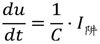
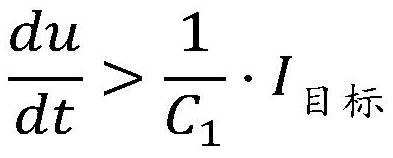
The invention relates to a semiconductor switch device (1) comprising a switchable power semiconductor (T2) and at least one regulating circuit (RS1, RS2) which comprises a current sink (S1, S2) and a current amplifier (V1,V2). The current sink (S1, S2) is capacitively coupled to the collector / drain of the power semiconductor (T2) via a regulating capacitor (C1) and is designed to discharge a partial current of the current flowing across the regulating capacitor (C1) during a switching process up to an adjustable maximum current. The input side of the current amplifier (V1, V2) is connected to the current sink (S1, S2) end capacitively coupled to the regulating capacitor (C1) and to a positive or a negative supply voltage, and the output side of the current amplifier is connected to the control electrode of the power semiconductor (T2). The current amplifier is designed such that the partial current of the current flowing across the regulating capacitor (C1) during the switching process that is not discharged by the current sink (S1, S2) is amplified and is fed to the control electrode of the power semiconductor (T2) such that the change in the voltage across the collector-emitter path or across the drain-source path of the power semiconductor (T2) is counteracted during a switching process. In order to improve the semiconductor switching device (1), the semiconductor switching device (1) additionally has an additional circuit (1.1) for an adapted activation transition, the circuit being connected to the control electrode of the power semiconductor (T2) and being designed for a smooth transition of the collector voltage or the drain voltage of the power semiconductor (T2) during a switchover of the collector-emitter path or drain-source path of the power semiconductor from an off state into an on state.

Description

technical field [0001] The invention relates to a semiconductor switching device comprising a switchable power semiconductor and an adaptive switching speed control for controlling the switching speed of the power semiconductor. Background technique [0002] Such semiconductor switching devices are used, for example, in frequency converters, which are used in drive technology, in which the switchable power semiconductors are designed as bipolar transistors (IGBTs) with insulated gate electrodes. However, the invention relates to all types of switchable power semiconductors. That is, power semiconductors having a base or gate, collector and emitter and also switchable semiconductors having gate, drain and source terminals. [0003] The switching speed of power semiconductors is usually selected according to two opposing criteria. On the one hand, in order to minimize switching losses, power semiconductors should be switched as fast as possible under the premise of safe oper...

Claims


Application Information

Patent Timeline
Patent Type & Authority Applications(China)
IPC IPC(8): H03K17/082H03K17/16
CPCH03K17/168H03K2217/0027H03K17/166H03K17/04H03K17/16
Inventor 巴斯蒂安·克鲁默安德烈亚斯·库纳特诺伯特·斯塔德特
Owner SIEMENS AG
Learn More