Color filter structure

A color filter and filter technology, applied in optics, optical components, nonlinear optics, etc., to achieve the effect of reducing the complexity of the process, the production cost, and the number of use

Inactive Publication Date: 2005-03-23
TPO DISPLAY
View PDF1 Cites 18 Cited by
  • Summary
  • Abstract
  • Description
  • Claims
  • Application Information

AI Technical Summary

Problems solved by technology

However, no matter using photosensitive resin material to make light-shielding layer or color filter, it is necessary to use corresponding photomask to precisely define its exposure position, so there are still certain restrictions on reducing the number of photomasks used.

Method used


Image

  • Color filter structure
  • Color filter structure
  • Color filter structure

Examples


Embodiment Construction

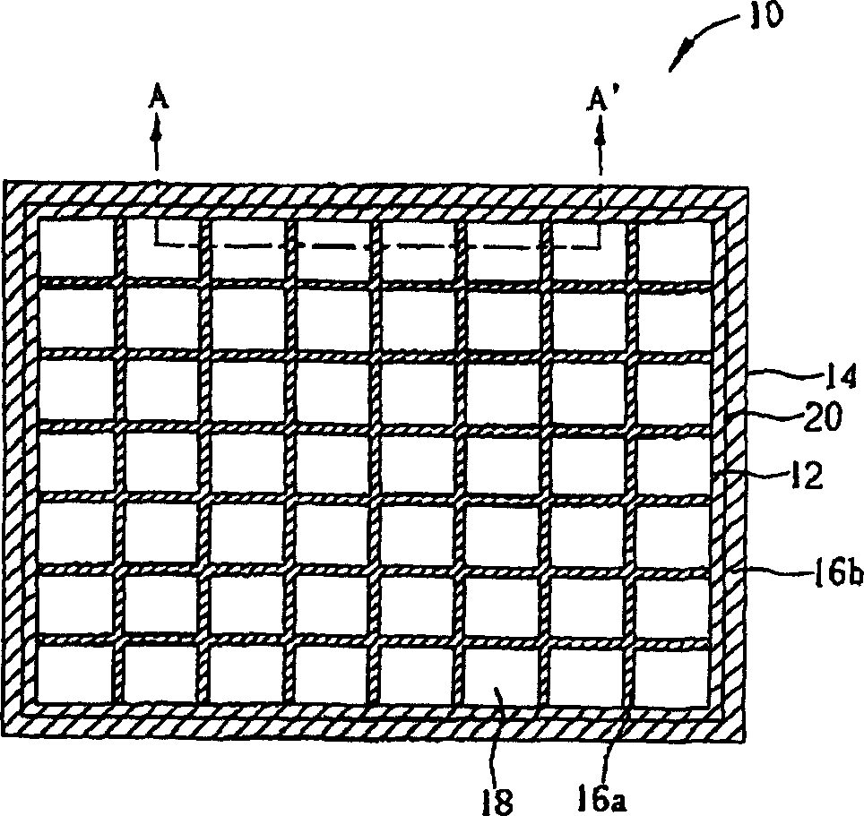
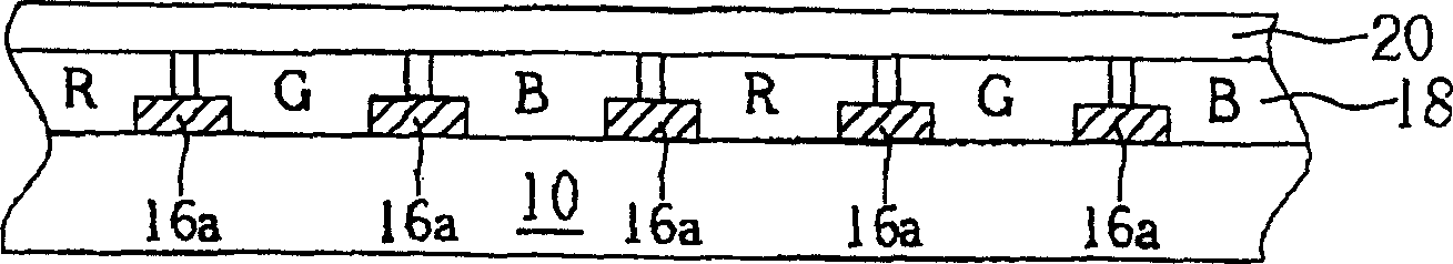
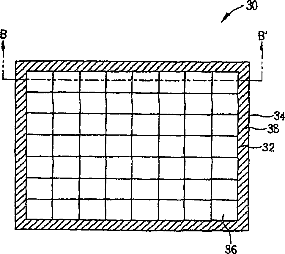
[0022] Please refer to image 3 and Figure 4 , image 3 It is a top view of a filter substrate of the present invention, Figure 4 for image 3 The schematic cross-sectional view of the filter substrate along the tangent line BB'. Such as image 3 and Figure 4 As shown, the filter substrate surface 30 defines a predetermined area 32 and a frame area 34 surrounding the predetermined area 32 . The predetermined area 32 is arranged in the center of the filter substrate 30 to correspond to the pixel area of ​​a thin film transistor substrate, and the predetermined area 32 includes a plurality of color filters 36 formed of conductive materials, such as red filter R, green filter G and blue filter B, etc., so that the light can pass through it to produce three primary colors such as red, green and blue, and then form a color image. They are all adjacent to each other or stacked on each other, so they can be further connected to form a conductive material layer, which can be...


PUM


Abstract

The invention discloses a colorful optical filtering chip structure, it includes a base board, a shading layer which is set in an area on the base board surface, and many electric optical filtering chips are set out of the frame on the base board surface to form a common electrode.

Description

technical field [0001] The present invention generally relates to a color filter structure, especially to a color filter structure of a liquid crystal display (LCD). Background technique [0002] The color filter structure of the existing liquid crystal display and the thin-film transistor (TFT) element used as the pixel driving circuit are respectively manufactured on two parallel and opposite glass substrates. Among them, the thin film transistor element is fabricated on the surface of the lower glass substrate (also known as thin film transistor substrate) by using multi-pass photolithography and etching process, while the color filter structure is fabricated on the upper glass substrate (also known as thin film transistor substrate) by photolithography or printing technology. Also known as the filter substrate) surface, so that each pixel of the liquid crystal display presents rich and bright colors. In the liquid crystal display process, a black matrix is ​​usually for...

Claims


Application Information

Patent Timeline
Patent Type & Authority Applications(China)
IPC IPC(8): G02B5/23G02F1/1335G02F1/1343
Inventor 郭光埌杨智胜
Owner TPO DISPLAY
Why Eureka
Try Eureka