Solid-state image sensor, manufacturing method for solid-state image sensor, and camera

A technology of a solid-state imaging device and a manufacturing method, which is applied in the direction of electric solid-state devices, semiconductor devices, instruments, etc., can solve problems such as shadows, shortening of the exit pupil distance, and image quality degradation, and achieve the reduction of shadows and shortening of the exit pupil distance. Effect

Inactive Publication Date: 2005-03-23
コラボイノベーションズインコーポレイテッド
View PDF1 Cites 6 Cited by
  • Summary
  • Abstract
  • Description
  • Claims
  • Application Information

AI Technical Summary

Problems solved by technology

[0007] However, according to the prior art described above, the reduction of the exit pupil distance has reached its limit in recent years for the thinning of video cameras for mobile phones and digital still cameras.
For example, for figure 1 structure, if the exit pupil distance is further shortened, then as figure 2 As shown, light cannot be collected on the light receiving element, and shadows are generated due to insufficient sensitivity at the end of the light receiving surface.
That is to say, the closer to the end from the center of the image, the worse the sensitivity, and the darker the image is to the periphery, and the image quality deteriorates.
[0008] Furthermore, due to the shortened exit pupil distance, the figure 2 In the case of the microlens, in order to form the microlens at an appropriate position, the mask must be positioned with higher precision in the process of forming the microlens, and the positioning is difficult to achieve in both design and manufacture.
[0009] And, although the solid-state imaging device of Japanese Unexamined Patent Publication No. 6-326284 can suppress the decrease in sensitivity when the aperture is opened wide, there is the same problem for shortening the exit pupil distance.

Method used


Image

  • Solid-state image sensor, manufacturing method for solid-state image sensor, and camera
  • Solid-state image sensor, manufacturing method for solid-state image sensor, and camera
  • Solid-state image sensor, manufacturing method for solid-state image sensor, and camera

Examples


no. 1 Embodiment approach

[0043]

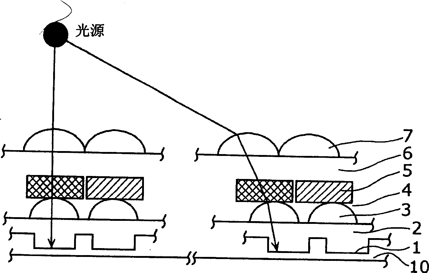
[0044] image 3 It is a cross-sectional view showing the solid-state imaging device according to the first embodiment of the present invention. This solid-state imaging device has a light-receiving surface composed of light-receiving elements (photodiodes) arranged two-dimensionally. This figure shows a cross section of two light receiving elements at the center (the left side of the figure) and a cross section of two light receiving elements at the end (right side of the figure) on the light receiving surface. In addition, the solid line in the figure indicates the source from the light source (equivalent to Figure 18 The incident light pattern of the lens 110) is shown.

[0045] In this figure, on a photodiode 1 formed on a silicon semiconductor substrate 10 of a solid-state imaging device, a planarized transparent insulating film (protective film) 2 made of BPSG (borophosphosilicate glass) or the like is sequentially stacked and formed. In-layer lens 3 with co...

no. 2 Embodiment approach

[0066]

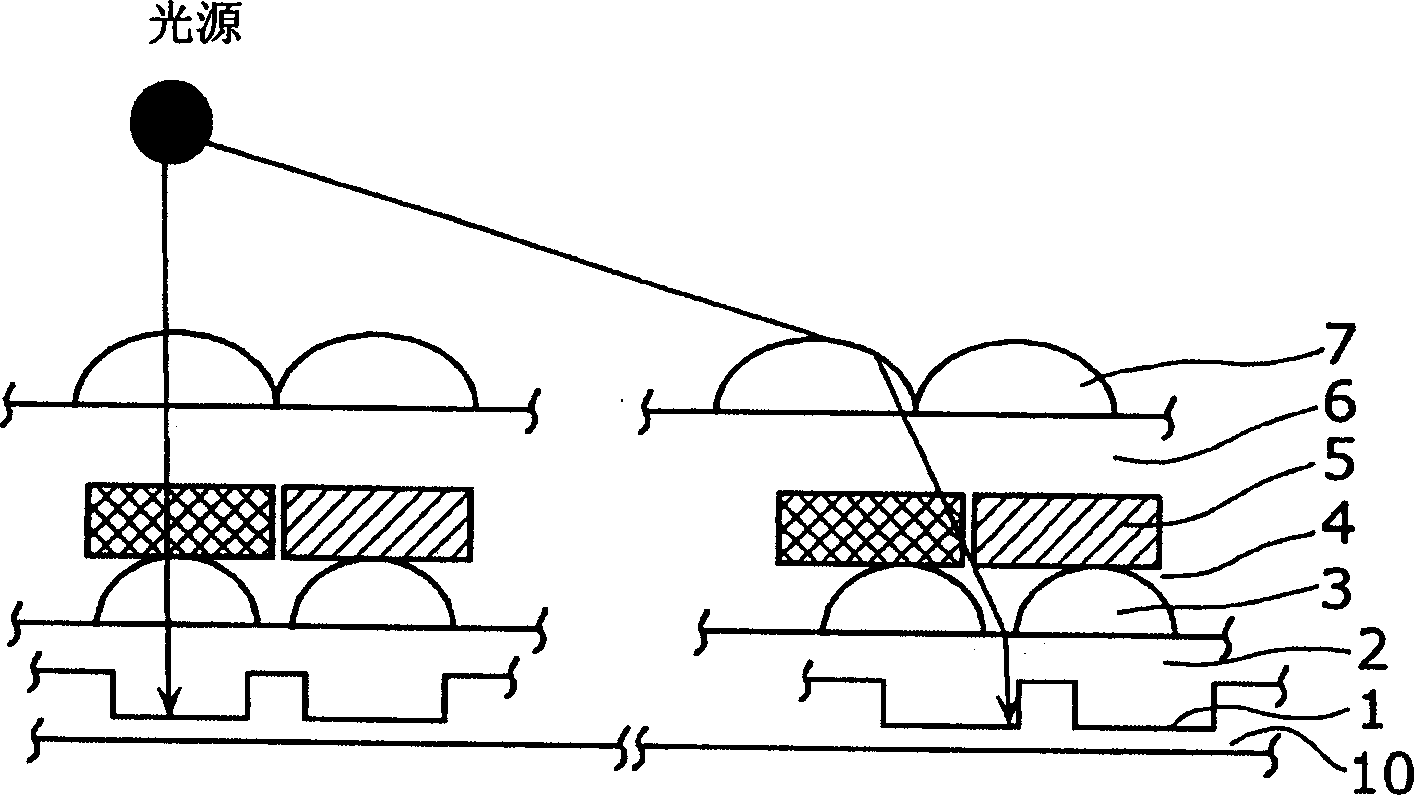
[0067] Figure 7 It is a cross-sectional view of the solid-state imaging device in the second embodiment of the present invention. The graph is structured with image 3 Compared with the above structure, the difference is that the color filter 5 is removed, and the microlens 7 is replaced by a microlens 7a. The description of the same points will be omitted below, and the description will focus on the different points.

[0068] The microlens 7 a is different from the microlens 7 in that it is opaque and doubles as a color filter.

[0069] According to this configuration, similar to the first embodiment, the exit pupil distance can be shortened and shadow shadows can be simulated. In addition, since the microlens 7a also serves as a color filter, the film thickness of the solid-state imaging device can be reduced by an amount equivalent to the thickness of the color filter layer. For example, in the solid-state imaging device in the first embodiment, when the dist...

no. 3 Embodiment approach

[0086]

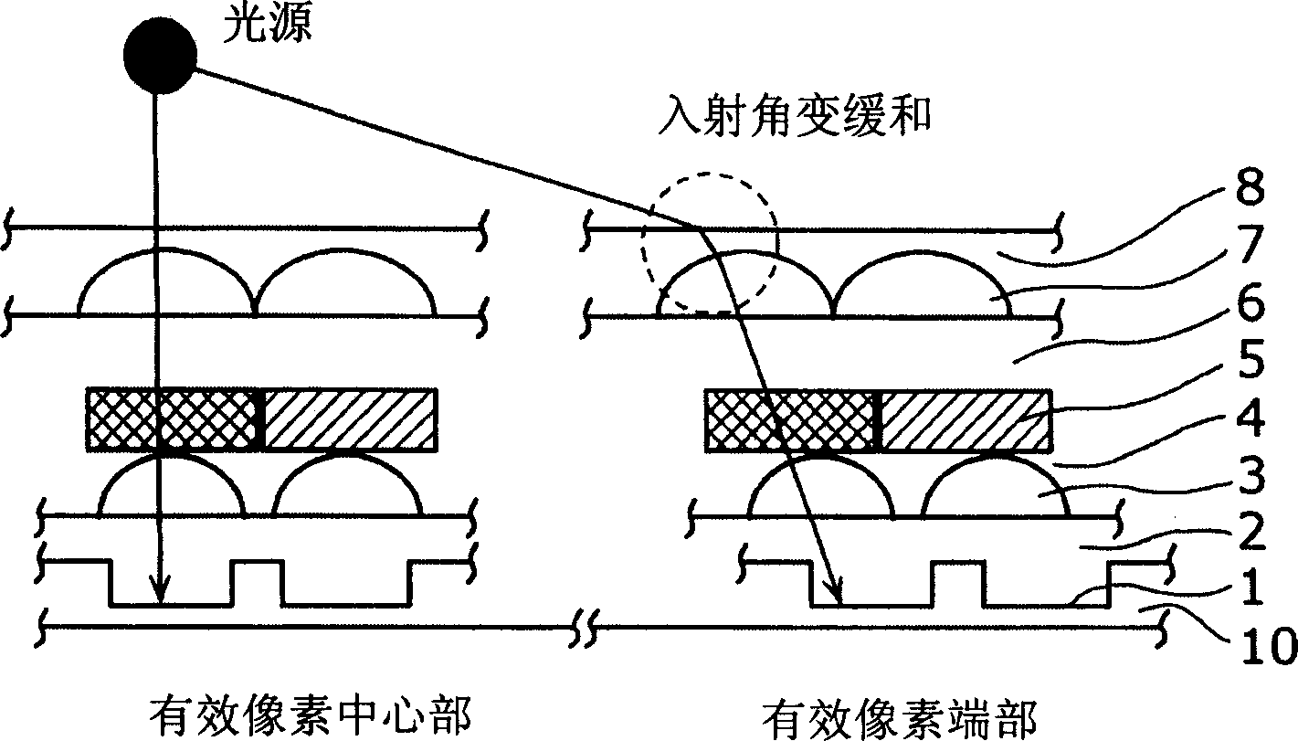
[0087] Figure 11 It is a cross-sectional view of the solid-state imaging device in the third embodiment of the present invention. The graph is structured with image 3 Compared with the above structure, the difference is that the color filter 5 is removed, and the inner lens 3 is replaced by the inner lens 3a. Hereinafter, the description of the same content is omitted, and the different content is mainly explained.

[0088]The in-layer lens 3 a is different from the in-layer lens 3 in that it is opaque and doubles as a color filter.

[0089] According to this configuration, similar to the first embodiment, the exit pupil distance can be shortened and shadow shadows can be simulated. In addition, since the in-layer lens 3a also serves as a color filter, the film thickness of the solid-state imaging device can be reduced by an amount equivalent to the thickness of the color filter layer. For example, in the solid-state imaging device in the first embodiment, whe...


PUM


Abstract

The solid-state image device in the present invention includes a plurality of light-receiving elements arranged in a light-receiving area, and a plurality of micro-lenses 7 corresponding to the light-receiving elements, and has a flattening film 8 formed on the plurality of the micro-lenses. At the center of the light-receiving area, micro-lenses 7 are placed in positions directly above the corresponding photodiodes 1, and placed in positions which are progressively offset from the positions directly above the corresponding photodiodes 1, towards the center of the light receiving area, as micro-lenses 7 are located farther from the center of the light-receiving area.

Description

technical field [0001] The present invention relates to a solid-state imaging device having microlenses on a plurality of light-receiving elements formed on a semiconductor substrate and a manufacturing method thereof. Background technique [0002] In recent years, while the number of pixels of solid-state imaging devices has increased, video cameras have also been miniaturized. [0003] In digital still cameras, camera-equipped mobile phones, and the like, the exit pupil distance has been shortened along with miniaturization of cameras. Here, the so-called exit pupil refers to the virtual image of the lens (or aperture) viewed from the light-receiving surface side, and the so-called exit pupil distance refers to the distance between the light-receiving surface and the lens (see Figure 18 ). [0004] Figure 18 A sectional view showing a camera portion of a mobile phone. A lens 110 is attached to a body 111 of the mobile phone, and a CCD image sensor 112 is provided insid...

Claims


Application Information

Patent Timeline
Patent Type & Authority Applications(China)
IPC IPC(8): G02B3/00H01L27/00H01L27/14H01L27/148H01L31/10H04N5/225H04N5/335H04N5/369
CPCH01L27/14621H01L27/14627H01L27/14806H01L27/14603H01L27/14H01L31/10
Inventor 酒勾宏小林正人寺西信一
Owner コラボイノベーションズインコーポレイテッド
Why Eureka
Try Eureka