
Semiconductor device and production method therefor

A manufacturing method and semiconductor technology, applied in semiconductor/solid-state device manufacturing, semiconductor devices, electrical components, etc., can solve problems such as affecting electron transport, reducing device channel conduction, and suppressing interface energy level well density.

Inactive Publication Date: 2005-03-23
PANASONIC CORP
View PDF0 Cites 15 Cited by
  • Summary
  • Abstract
  • Description
  • Claims
  • Application Information

AI Technical Summary

Problems solved by technology

For example, in a thermally oxidized film with a thickness of 40nm formed on the 4H-SiC (0001) surface, the interface level well density is suppressed to 5×10 11 [cm -2 eV -1 ] The following is very difficult
[0008] This interface energy level well will greatly affect electron transport and significantly reduce the channel conduction of the device

Method used


Image

  • Semiconductor device and production method therefor
  • Semiconductor device and production method therefor
  • Semiconductor device and production method therefor

Examples


no. 1 approach

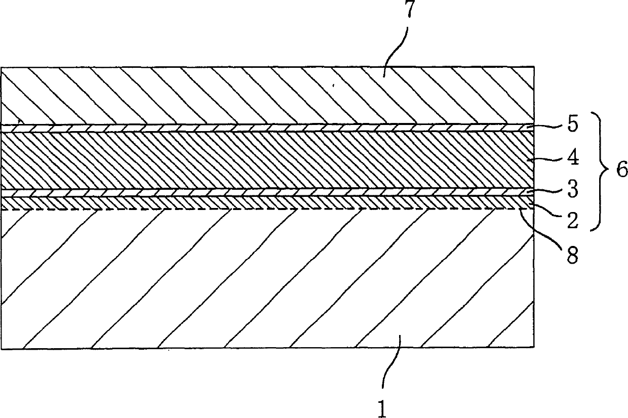
[0066] In this embodiment mode, a case where a first insulating film obtained by thermal oxidation of SiC and a second insulating film deposited by CVD or the like is formed as a gate insulating film of MISFET or the like will be described.

[0067] (Investigation by inventors etc.)

[0068] It is generally considered that when a silicon carbide MISFET is used in a low-loss power semiconductor device, a gate insulating film having a thickness of approximately 150 nm or more should be formed on silicon carbide.

[0069] However, this causes carbon to remain in the oxide film formed by thermal oxidation treatment on silicon carbide, and particularly, a high concentration of carbon remains in the vicinity of the interface with silicon carbide in the oxide film. Since the existence of such carbon is a cause of defects, the composition ratio of the transition layer should be changed more drastically from the gate insulating film side to the silicon carbide side.

[0070] Here, in ...

no. 2 approach

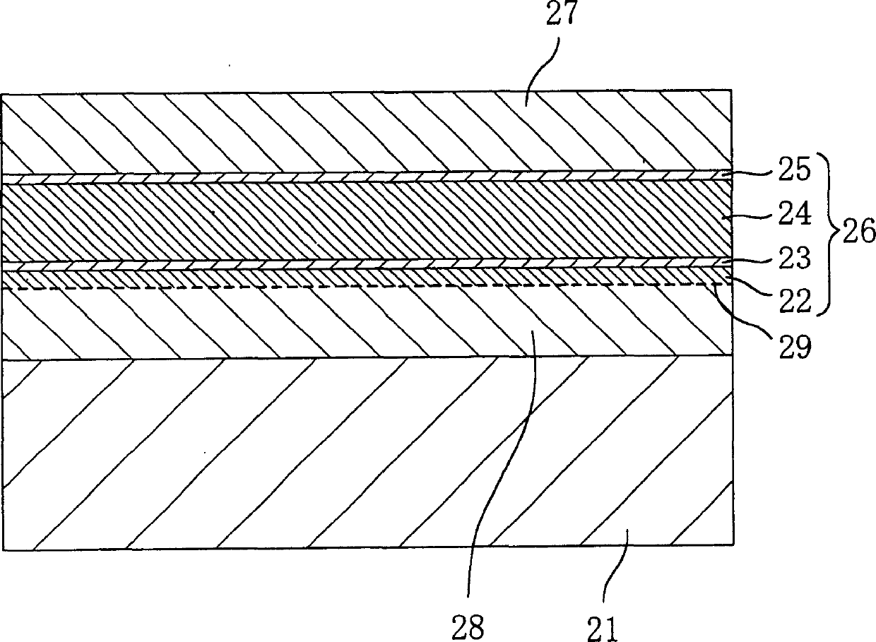
[0113] In this embodiment mode, an example in which the gate insulating film considered in the first embodiment mode is applied to a storage-enhanced insulated gate semiconductor device will be described.

[0114] Next, the structure near the gate insulating film in the semiconductor device according to the second embodiment of the present invention will be described with reference to FIG. 4 . 4 is a cross-sectional view showing a structure near a gate insulating film in a semiconductor device in a second embodiment.

[0115] As shown in FIG. 4, in the semiconductor device of the present invention, an n-type channel region 28 is formed on the top of the p-type SiC layer 21, and a gate insulating film 26 is formed thereon, which is a thermal oxide film with a thickness of about 5 nm. A first insulating film 22, an oxynitride film having a thickness of about 5 nm, that is, the first cover layer 23, a deposited oxide film having a thickness of about 130 nm, that is, the second in...

no. 3 approach

[0120] In this embodiment mode, an example in which the gate insulating film in the first embodiment mode is applied to an insulated gate type semiconductor device having a δ-doped layer will be described.

[0121] This embodiment mode is characterized in that the gate insulating film described in the first embodiment mode is formed on the δ-doped layer. Since the structure of this gate insulating film is the same as that of the first embodiment, description thereof will be omitted.

[0122] FIG. 8 is a cross-sectional view showing the structure of the semiconductor device in the third embodiment.

[0123] As shown in FIG. 8 , the semiconductor device of this embodiment includes an n-type SiC substrate 40 , a p-type SiC layer 41 formed on the SiC substrate 40 , and a channel region having a δ-doped layer formed on the top of the p-type SiC layer 41 . 46. ​​The gate insulating film 47 formed on the channel region 46, the gate electrode 48 formed on the gate insulating film 47,...


PUM

PropertyMeasurementUnit
Thicknessaaaaaaaaaa
Thicknessaaaaaaaaaa
Thicknessaaaaaaaaaa

Abstract

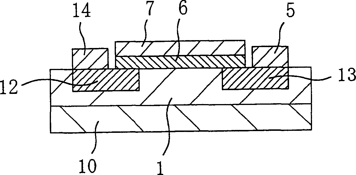
An upper part of a SIC substrate 1 is oxidized at a temperature of 800 to 1400 DEG C., inclusive, in an oxygen atmosphere at 1.4x10<2>Pa or less, thereby forming a first insulating film 2 which is a thermal oxide film of 20 nm or less in thickness. Thereafter, annealing is performed, and then a first cap layer 3, which is a nitride film of about 5 nm in thickness, is formed thereon by CVD. A second insulating film 4, which is an oxide film of about 130 nm in thickness, is deposited thereon by CVD. A second cap layer 5, which is a nitride film of about 10 nm in thickness, is formed thereon. In this manner, a gate insulating film 6 made of the first insulating film 2 through the second cap layer 5 is formed, thus obtaining a low-loss highly-reliable semiconductor device.

Description

technical field [0001] The invention relates to a semiconductor device with a SiC layer and a manufacturing method thereof, in particular to an insulated gate type semiconductor device and a manufacturing method thereof. Background technique [0002] Silicon carbide has high dielectric breakdown characteristics even compared to other semiconductor materials with a wide band gap. Therefore, application to low-loss power devices has been expected in recent years. [0003] A high-quality silicon dioxide film can be formed on silicon carbide by performing thermal oxidation treatment on the upper part of silicon carbide. Therefore, in order to form a silicon carbide semiconductor device for high-power driving, it is considered to be effective to use an insulated gate type semiconductor device form. [0004] When MISFETs using silicon carbide are used in low-loss power semiconductor devices, it is necessary to reduce the density of interface level wells located in the interface ...

Claims


Application Information

Patent Timeline
IPC IPC(8): H01L21/04H01L21/28H01L29/24H01L29/417H01L29/51H01L29/78
CPCH01L21/28185H01L21/049H01L21/28202H01L29/1608H01L29/41766H01L29/513H01L29/518H01L29/66068H01L29/78H01L29/7802H01L29/7838
Inventor 山下贤哉北畠真高桥邦方楠本修内田正雄宫永良子
Owner PANASONIC CORP
Learn More