Plasma display panel

A plasma and display panel technology, applied in alternating current plasma display panels, gas discharge electrodes, solid cathode parts, etc., can solve the problem of damaging electrodes

Inactive Publication Date: 2005-05-04
SAMSUNG SDI CO LTD
View PDF0 Cites 4 Cited by
  • Summary
  • Abstract
  • Description
  • Claims
  • Application Information

AI Technical Summary

Problems solved by technology

[0006] In DC type PDP, since the charge moves directly between the corresponding electrodes, it can seriously damage the electrodes

Method used


Image

  • Plasma display panel
  • Plasma display panel
  • Plasma display panel

Examples


Embodiment Construction

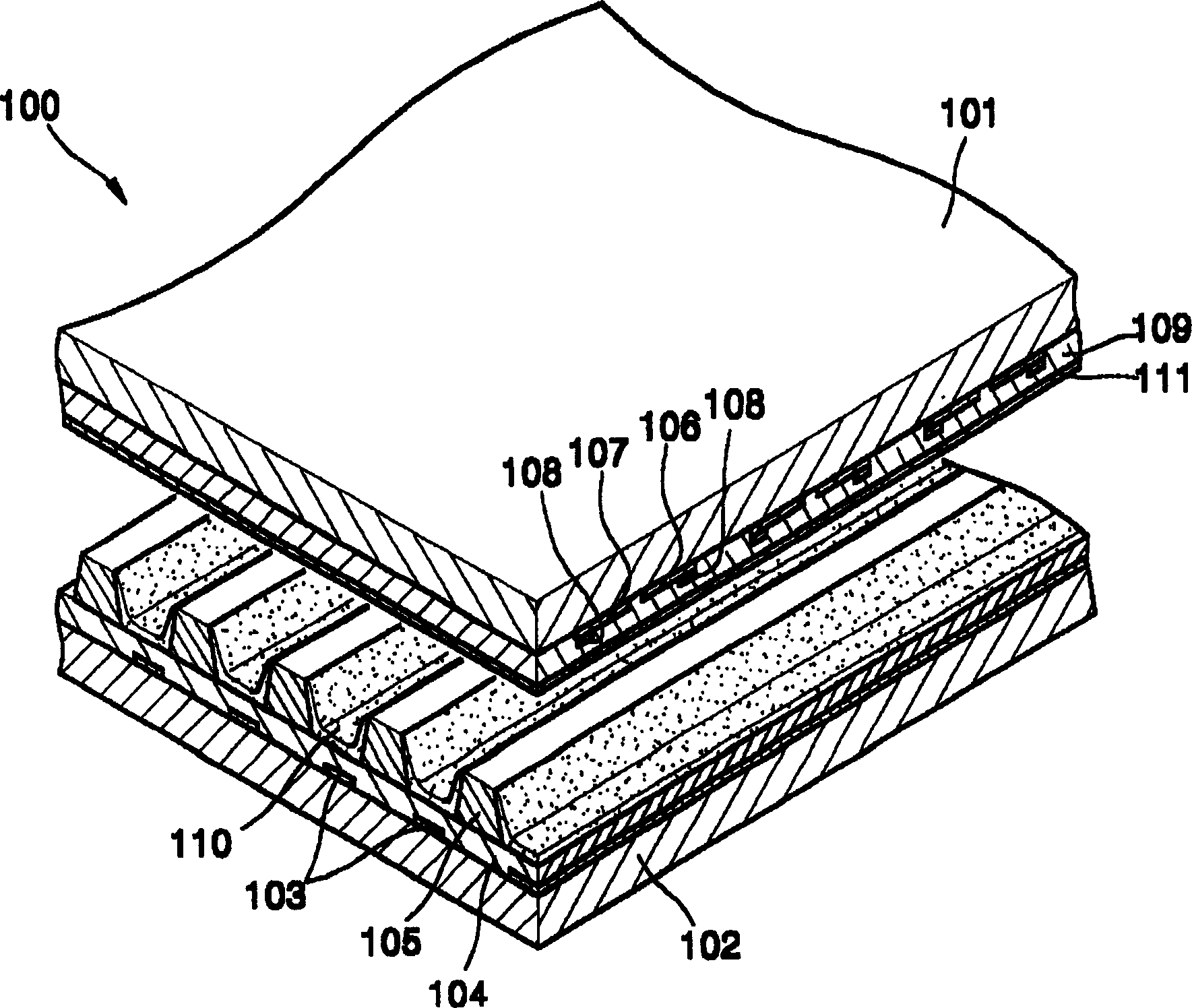
[0060] Such as figure 1 As shown, a conventional surface discharge PDP 100 including an AC-type three-electrode surface discharge PDP includes a front substrate 101 through which visible light is emitted from a phosphor 110 in a discharge space, X and Y electrodes 107 and 108 are adapted to generate a discharge, bus electrodes 108 and the dielectric layer 109 and protective layer sequentially formed thereon are all disposed on the front substrate 101, thereby reducing the transmittance of visible light to about 60%. Also, in the conventional surface discharge PDP 100, the discharge electrode is formed on the top of the discharge space, that is, on the inner surface of the front substrate 101 through which visible light passes, and a discharge is generated on the inner surface to scatter visible light, by This lowers the luminous efficiency. Also, if the conventional PDP 100 is used for an extended period of time, charged particles in the discharge gas may sputter ions onto th...


PUM


Abstract

A plasma display panel includes a pair of substrates (201;202) spaced apart from each other and facing each other, a visible light generator (210) arranged between the pair of substrates (201;202), and an electrode layer (206) adapted to apply the same potential to a plane arranged between the pair of substrates (201;202) at a predetermined angle with respect to a direction perpendicular to the pair of substrates (201;202).

Description

[0001] Pursuant to 35 U.S.C. §119, this application claims priority to a prior application "Plasma Display Panel" filed on October 29, 2003 with the Korean Intellectual Property Office and assigned Serial No. 2003-76096. The content of this application is incorporated herein by reference. technical field [0002] The present invention relates to a plasma display panel (PDP) suitable for displaying characters or images using a gas discharge phenomenon, and more particularly to a PDP having an increased surface on which discharge is generated. Background technique [0003] In recent years, PDPs have attracted considerable attention as the most promising next-generation flat panel display devices because of their various favorable features, including high image quality display, very thin and lightweight design, and wide range of viewing angles, and they can be manufactured in a simple manner and can easily be manufactured in large sizes. [0004] Such PDPs are roughly classifi...

Claims


Application Information

Patent Timeline
Patent Type & Authority Applications(China)
IPC IPC(8): H01J11/14H01J11/16H01J11/22H01J11/24H01J11/26H01J11/32H01J11/34H01J11/36
CPCH01J11/24H01J11/32H01J11/36H01J11/16H01J2211/323H01J2211/245
Inventor 禹锡均姜景斗李源朱
Owner SAMSUNG SDI CO LTD
Why Eureka
Try Eureka