Wafer radiating element

A technology for heat-dissipating components and wafers, which is applied to electrical components, electrical solid-state devices, semiconductor devices, etc., and can solve problems such as affecting the filling process time.

Inactive Publication Date: 2005-06-01
SILICON INTEGRATED SYSTEMS
View PDF0 Cites 6 Cited by
  • Summary
  • Abstract
  • Description
  • Claims
  • Application Information

AI Technical Summary

Problems solved by technology

However, although there are known methods to reduce the injection speed of the molding resin 191 to reduce the probability of the air holes 193, it will affect the overall filling process time.

Method used


Image

  • Wafer radiating element
  • Wafer radiating element
  • Wafer radiating element

Examples


Embodiment Construction

[0024] The present invention is mainly a chip cooling element, which will be described in detail below. The embodiment of the present invention is mainly to solve the problems described in the prior art, but the patent scope of the present invention is not limited to the following figures and descriptions of the embodiments, but should be based on the scope and spirit of the applied patent allow.

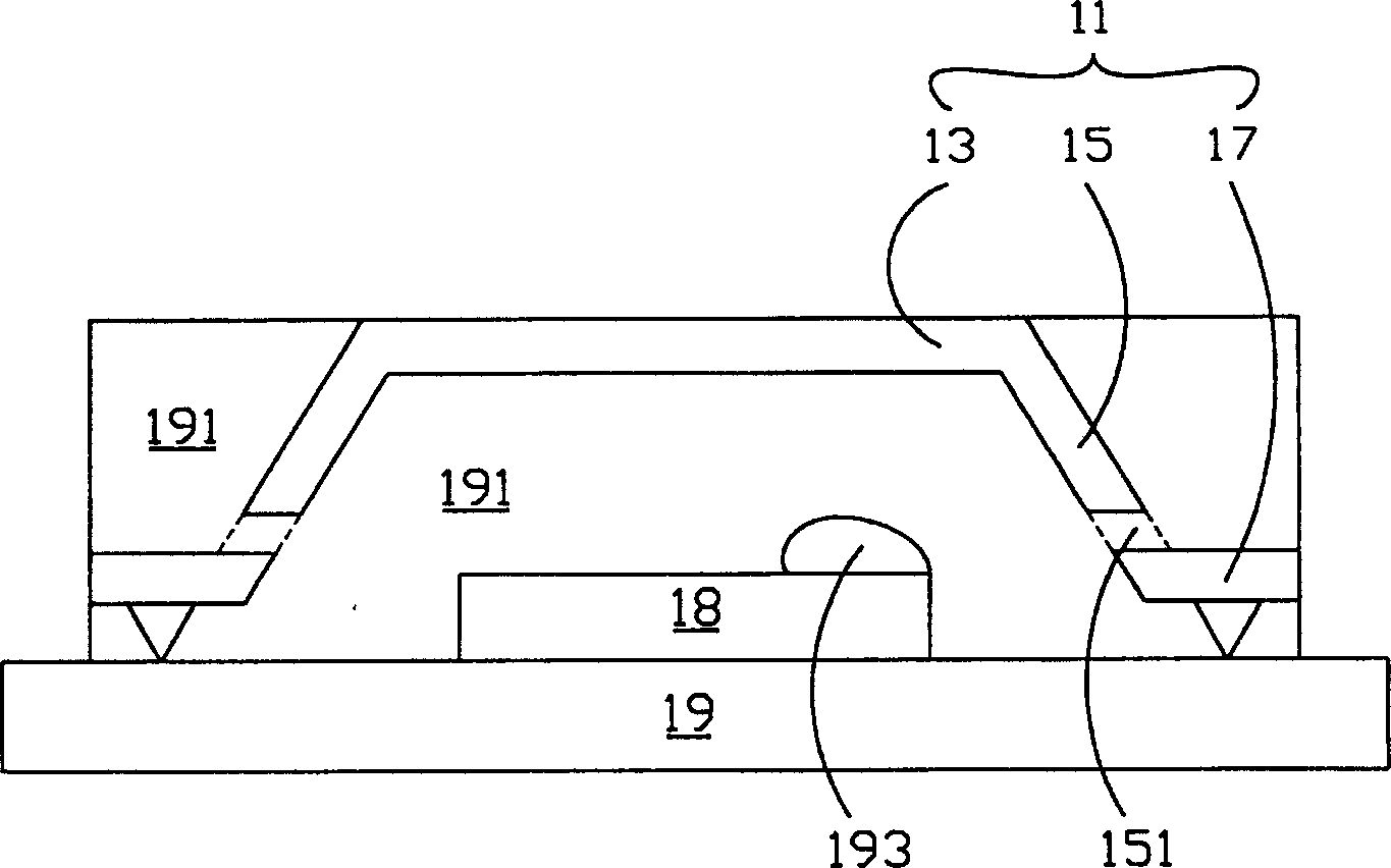
[0025] The first embodiment of the wafer cooling element 21 of the present invention is as figure 2 As shown, there is a top plate 23, side walls 25 and bottom plate 27. The top plate 23 is bent and extended to connect to the side wall 25 , and the side wall 25 is bent and extended to connect to the bottom plate 27 . The top plate 23 has a recessed plate portion 235 .

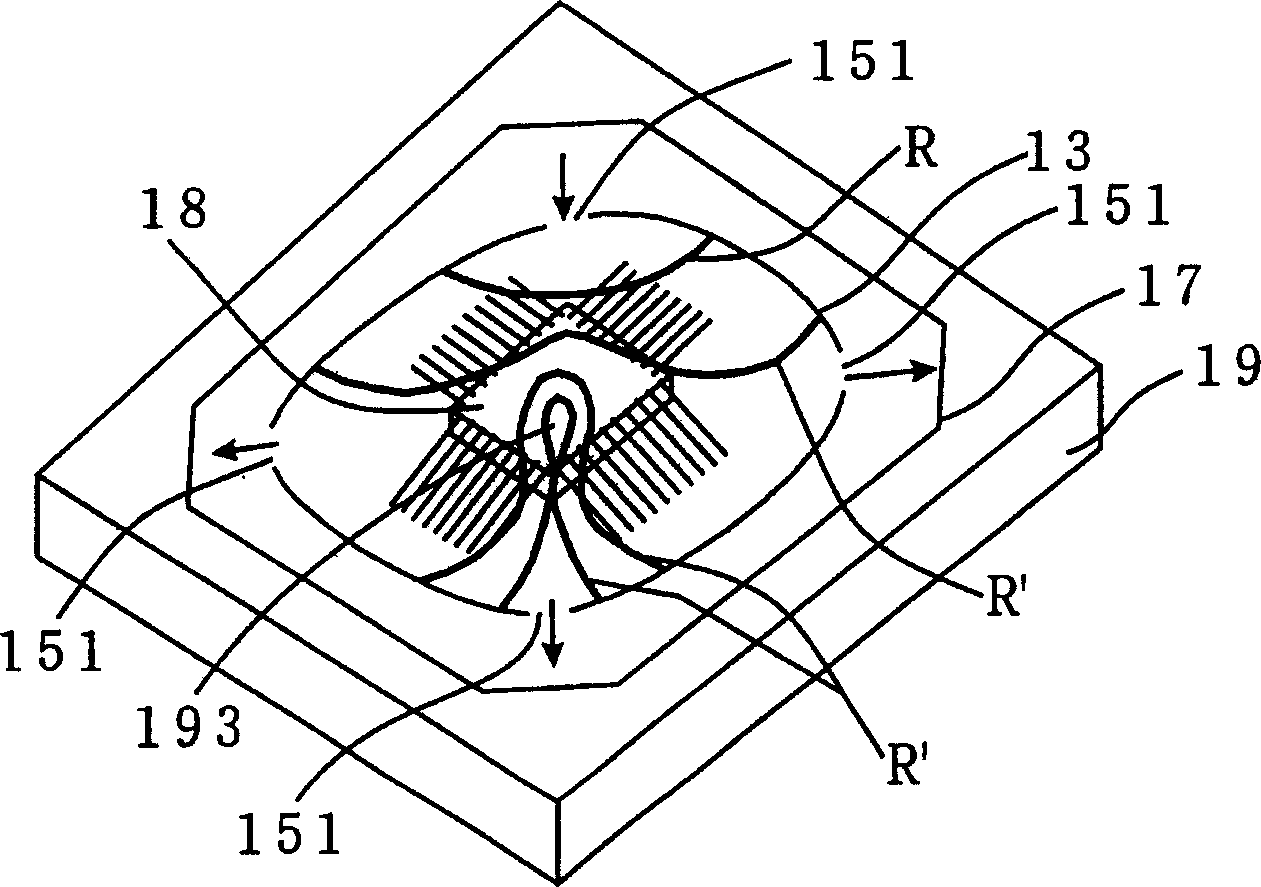
[0026] Such as image 3 As shown, the chip cooling element 21 is applied on a chip 33 , contacts and is fixed on part of the chip 33 through the concave plate portion 235 , and the bottom plate 27 is fixed on th...


PUM


Abstract

The chip heat radiating element is for chip to radiate heat. The chip heat radiating element has one top plate and side walls, and the top plate is bent and extended to connected side walls and has notched part to contact with chip.

Description

technical field [0001] The present invention relates to a chip cooling element, in particular to a chip cooling element using a recessed plate portion. Background technique [0002] Generally, the heat sink and the surface of the chip in the chip package assembly will be separated by molding resin (Epoxy Molding Compound, EMC), so as to use the molding resin to protect each circuit connected between the chip and the substrate to prevent short circuit. However, because the heat dissipation properties of the molding resin are not good, the heat dissipated by the heat source cannot be dissipated properly through the molding resin, and then the reliability of the chip package assembly is likely to be shortened. [0003] Such as Figure 1A As shown, the known chip package assembly 11 structure is applied to a chip 18 . The wafer cooling element 11 has a top plate 13 , a side wall 15 and a bottom plate 17 . The top plate 13 is bent and extended to connect to the side wall 15 , a...

Claims


Application Information

Patent Timeline
Patent Type & Authority Applications(China)
IPC IPC(8): H01L23/367
CPCH01L2924/181H01L2924/1815H01L2924/00012
Inventor 刘渭琪林蔚峰吴忠儒
Owner SILICON INTEGRATED SYSTEMS
Why Eureka
Try Eureka