
Smear evaluation circuit, image pickup apparatus and method of driving solid-state image sensor

A technology of solid-state imaging components and computing circuits, applied in the direction of electric solid-state devices, electrical components, circuits, etc., can solve problems such as reducing power consumption, and achieve the effects of ensuring frame rate, reducing the number of lines, and reducing the size

Inactive Publication Date: 2005-06-01
SANYO ELECTRIC CO LTD
View PDF0 Cites 10 Cited by
  • Summary
  • Abstract
  • Description
  • Claims
  • Application Information

AI Technical Summary

Problems solved by technology

From this point of view, it is necessary to use Figure 19 There is room for reduction of power consumption in the existing technology of the circuit operation

Method used


Image

  • Smear evaluation circuit, image pickup apparatus and method of driving solid-state image sensor
  • Smear evaluation circuit, image pickup apparatus and method of driving solid-state image sensor
  • Smear evaluation circuit, image pickup apparatus and method of driving solid-state image sensor

Examples


Embodiment approach 1

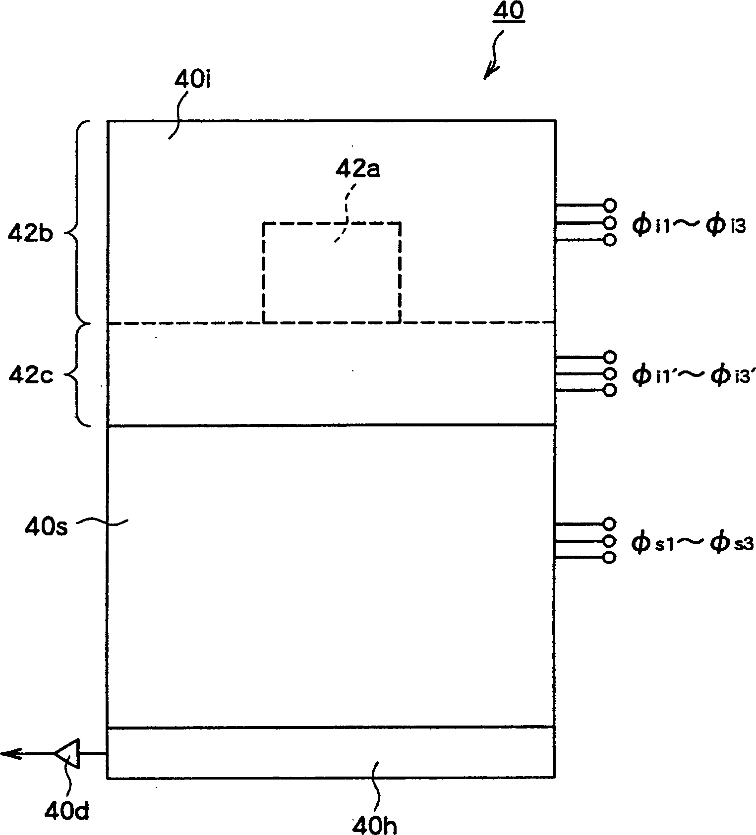
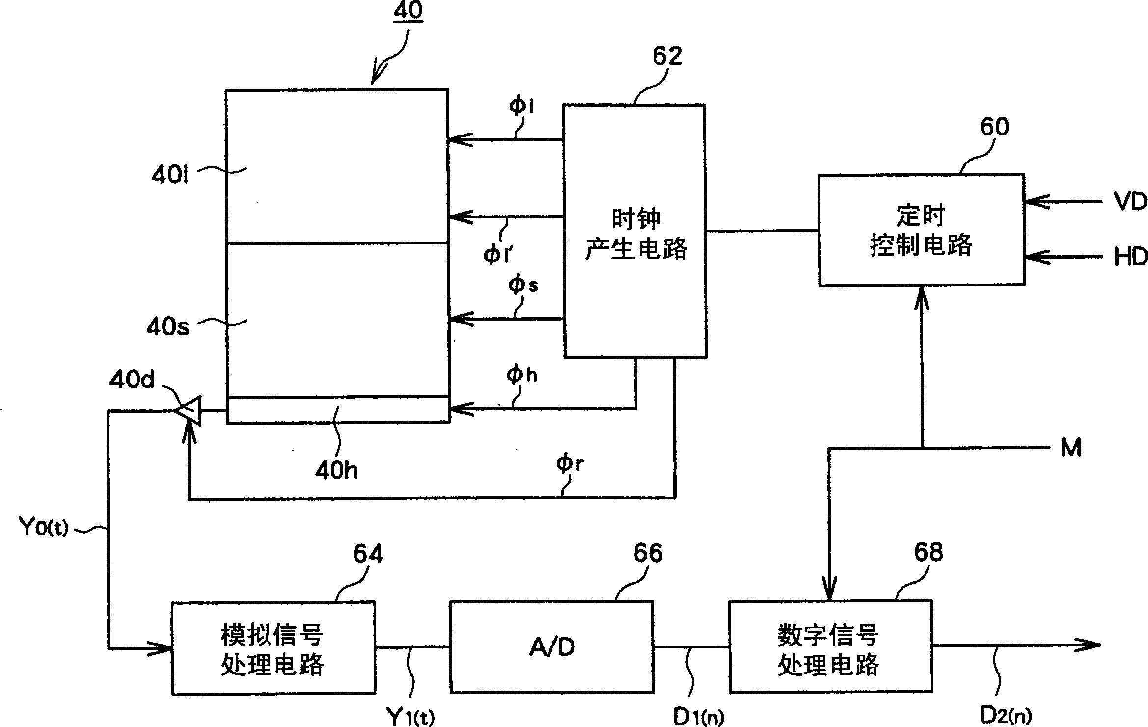
[0072] figure 1 It is a schematic plan view of a frame transfer type CCD image sensor according to an embodiment of the present invention. The image sensor 40 includes an imaging portion 40i, a storage portion 40s, a horizontal transfer portion 40h, and an output portion 40d formed on the surface of the semiconductor substrate. The image sensor 40 is used, for example, to capture a high-resolution still image using all the units of the imaging unit 40i. On the other hand, when such a resolution is not required, it can also be used for magnifying and displaying the central portion of the image captured by the imaging unit 40i. In addition, the imaging of only the image of the center part of the imaging part 40i is suitable for displaying on a preview screen, imaging a moving image, or the like.

[0073] In the imaging section 40i, a plurality of cells that generate signal charges corresponding to the amount of incident light are arranged in rows and columns. In this embodim...

Embodiment approach 2

[0109] The structure of the imaging device according to the second embodiment of the present invention is basically the same as that of the above-mentioned first embodiment. In the following description, reference is made to Figure 1 to Figure 5At the same time, the same symbols are assigned to the constituent elements with the same functions, so as to realize the brevity of the description. The main feature of this apparatus is the driving method of the image sensor 40 in the image extraction mode. The image sensor 40 of the present camera device can drive the vertical CCD shift register of the front readout area 42c and the vertical shift register of the area 42b, respectively. This makes it possible to selectively perform the operation of reading out the signal charges stored in the first to mth lines (the front readout area 42c) of the imaging unit 40i as image signals (the offset area readout operation) and the (mth) readout operation. The operation of reading out the s...

Embodiment approach 3

[0119] In the description of the third embodiment of the present invention, the same reference numerals are added to the same components as those of the above-described first and second embodiments to simplify the description.

[0120] Figure 9 It is a schematic plan view of the frame transfer type CCD image sensor which concerns on embodiment of this invention. As the image sensor of the present device, the above-described image sensor 40 capable of driving the front readout area 42c independently of the area 42b can be used, but in this embodiment, a set of three-phase clocks φi1 to φi3 is used for vertical alignment of the imaging section. The transmitted image sensor 120 . The basic structure of the image sensor 120 and the description of the prior art Figure 15 The general frame transfer type CCD image sensor shown is the same, and the vertical CCD shift registers of the imaging section and storage section have Figure 16 The schematic partial cross-sectional view sho...


PUM


Abstract

The problem to be solved by the present invention is to increase the frame rate while suppressing smearing in the case of using images of partial regions in a frame transfer type CCD pattern sensor. A smear calculation circuit (100) obtains a smear component of an image signal V(j) of each line in a central area to be image extracted from an accumulated value of image signals of preceding lines. Here, the application of the smear component from the preceding readout area prior to the central area is not performed by accumulation of image signals in the preceding readout area, but is estimated based on image signals in the line preceding the central area. This estimated value is set in the line memory (106) as an initial value of the smear component, and accumulation processing for each line in the central area is started. Thus, the readout of the image signal in the previous readout area is omitted, and the frame rate is improved.

Description

technical field [0001] The present invention relates to a smear arithmetic circuit, an imaging device, and a driving method of a solid-state imaging element for obtaining a smear component that can be included in an image signal of a frame transfer CCD image sensor. Background technique [0002] In an imaging device that generates an image signal using a solid-state imaging element or the like, image magnification can be performed not only by optical zooming (optical zooming) using a lens, but also by zooming (digital zooming) by signal processing. In particular, in an imaging device using a solid-state imaging element, as the number of pixels of the solid-state imaging element increases, a sufficient resolution can be obtained even when digital zooming is performed. [0003] Conventionally, digital zoom has been realized by reading out the signal charges of all the pixels of the imaging section of the solid-state imaging element as an image signal, and signal-processing a p...

Claims


Application Information

Patent Timeline
Patent Type & Authority Applications(China)
IPC IPC(8): H01L27/148H04N1/40H04N5/335H04N5/341H04N5/359H04N5/369H04N5/3725H04N9/64
CPCH01L27/148H04N1/40H04N9/646H04N25/443H04N25/625H04N25/72
Inventor 松山久
Owner SANYO ELECTRIC CO LTD
Learn More