Display device, driving method thereof, and element substrate

A technology for display devices and light-emitting elements, which is applied to electrical components, lighting devices, static indicators, etc., to achieve the effects of suppressing changes in current values, high image quality, and reducing defects

Inactive Publication Date: 2005-06-08
SEMICON ENERGY LAB CO LTD
View PDF1 Cites 17 Cited by
  • Summary
  • Abstract
  • Description
  • Claims
  • Application Information

AI Technical Summary

Problems solved by technology

As a result, the value of the current flowing in the driving TFT is changed, resulting in an inverted gray scale of a screen image having a gray scale, etc.

Method used


Image

  • Display device, driving method thereof, and element substrate
  • Display device, driving method thereof, and element substrate
  • Display device, driving method thereof, and element substrate

Examples


Embodiment 1

[0080] The structure of the light emitting element as a component of the present invention is explained below. The light emitting element has a laminated structure of a conductive layer, an electroluminescent layer, and a conductive layer formed over a substrate having an insulating surface composed of glass, quartz, metal, organic material, or the like. The light-emitting element may be a stacked type including an electroluminescent layer formed of a plurality of layers, a single-layer type including an electroluminescent layer formed of a single layer, or a layered type including an electroluminescent layer formed of a multilayer with unclear boundaries. mixed types. Moreover, the light-emitting element can adopt any one of the following two structures according to the direction of light emission, that is, a forward stacked structure in which a conductive layer corresponding to the anode, an electroluminescent layer, and a conductive layer corresponding to the cathode are st...

Embodiment 2

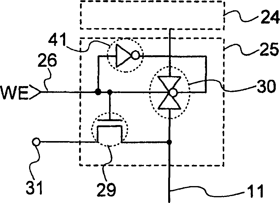
[0085] The structure of a tri-state buffer as an example of the components of the present invention is explained below. The tri-state buffer includes NAND 81, NOR 82, inverter 83, P-type TFT 84 and N-type TFT 85 ( Figure 6A ). One of the two input nodes of the NAND 81 is connected to the selection signal line 26, and the other node is connected to the shift register. That is, one of the two input nodes of the NAND 81 is input with a WE signal, and the other node is input with a pulse. One of the two input nodes of the NOR 82 is connected to the selection signal line 26 through the inverter 83, and the other node is connected to the shift register. That is, one of the two input nodes of the NOR 82 is input with an inverted WE signal, and the other is input with a pulse. The source electrode of the P-type TFT 84 is connected to a high-potential power supply 86 , while the source electrode of the N-type TFT 85 is connected to a low-potential power supply 87 .

[0086] Accord...

Embodiment 3

[0090] The time gray scale method employed in the display device of the present invention, that is, the driving method (operation) of the display device of the present invention is explained below. The description will be made with reference to a timing chart in which the ordinate represents the scanning line and the abscissa represents the time, and a timing chart of the gate line Gi in the i-th row (1≤i≤n) ( Figure 7A and 7B ). The frame frequency is about 60Hz, and the time period for writing to the screen at one time is called the frame period. According to this time grayscale method, one frame period is divided into a plurality of subframe periods. The number of divisions is usually equal to the number of grayscale bits, and this is shown in this embodiment.

[0091] noticed that in Figure 7A and 7B The timing diagram shown in is just an example, and the subframe period may be further divided in order to reduce pseudo contours and the like.

[0092] First, describ...


PUM


Abstract

The present invention provides a display device having high image quality and high resolution, a driving method thereof, and an element substrate. Also, the present invention provides a display device having improved degradation of light emitting elements, a driving method thereof, and an element substrate. The display device of the present invention has a first transistor, a second transistor, a third transistor, a light emitting element, a source driver, a first gate driver, and a second gate driver. A gate electrode of the first transistor is connected to a gate line, one of a source electrode and a drain electrode thereof is connected to a source line, and the other is connected to a gate electrode of the third transistor. The light emitting element, the second transistor and the third transistor are connected in series between the first power source and the second power source. The gate electrode of the second transistor is connected to a third power supply, the source driver is connected to the source line, and the first gate driver and the second gate driver are connected to the gate line.

Description

technical field [0001] The present invention relates to a display device with self-luminous elements and a driving method thereof, and an element substrate with elements on an insulating surface. Background technique [0002] In recent years, display devices having self-luminous elements typified by electroluminescent elements have been researched and developed, and it is desired to widely utilize the characteristics of self-luminous types, such as high image quality, wide viewing angle, thinness and light weight, and do not require backlight. A feature of a display device having a light emitting element is that signals are written to pixels of a plurality of different stages during one gate signal line selection period (for example, see Patent Document 1). [0003] [Patent Document 1] Japanese Patent Laid-Open No. 2001-324958 [0004] In the pixel circuit disclosed in Patent Document 1, when the potentials of source lines, gate lines, etc. adjacent to each other change, t...

Claims


Application Information

Patent Timeline
Patent Type & Authority Applications(China)
IPC IPC(8): G09G3/20G09G3/32H01L27/32H05B44/00
CPCG09G3/2022G09G3/32G09G2300/0809G09G2300/0842G09G2310/0251G09G2310/0256G09G2310/0267G09G2310/0275G09G2320/043G09G2330/08H10K59/12H10K2102/3031
Inventor 长尾祥木村肇安西彩山崎优纳光明棚田好文
Owner SEMICON ENERGY LAB CO LTD
Why Eureka
Try Eureka