Liquid crystal display device and manufacturing method thereof

A liquid crystal display device and liquid crystal layer technology, applied in transistors, static indicators, optics, etc., can solve problems such as crosstalk, decrease in pixel aperture ratio, panel scrapping, etc., and achieve the effect of increasing the aperture ratio and improving the good rate of products

Active Publication Date: 2005-06-29
AU OPTRONICS CORP
View PDF0 Cites 5 Cited by
  • Summary
  • Abstract
  • Description
  • Claims
  • Application Information

AI Technical Summary

Problems solved by technology

[0006] However, the above-mentioned known LCDs have many disadvantages
For example, when the Cs line 120 breaks 190, it will cause horizontal bright lines or dark lines and affect the display quality, so the panel needs to be scrapped
Also, since the laterally extending Cs lines 120 are opaque, the aperture ratio of the pixel will be reduced.
In addition, cross talk may occur at the intersection of the Cs line 120 and the source line 150, thereby affecting the display quality.

Method used


Image

  • Liquid crystal display device and manufacturing method thereof
  • Liquid crystal display device and manufacturing method thereof
  • Liquid crystal display device and manufacturing method thereof

Examples


no. 1 example

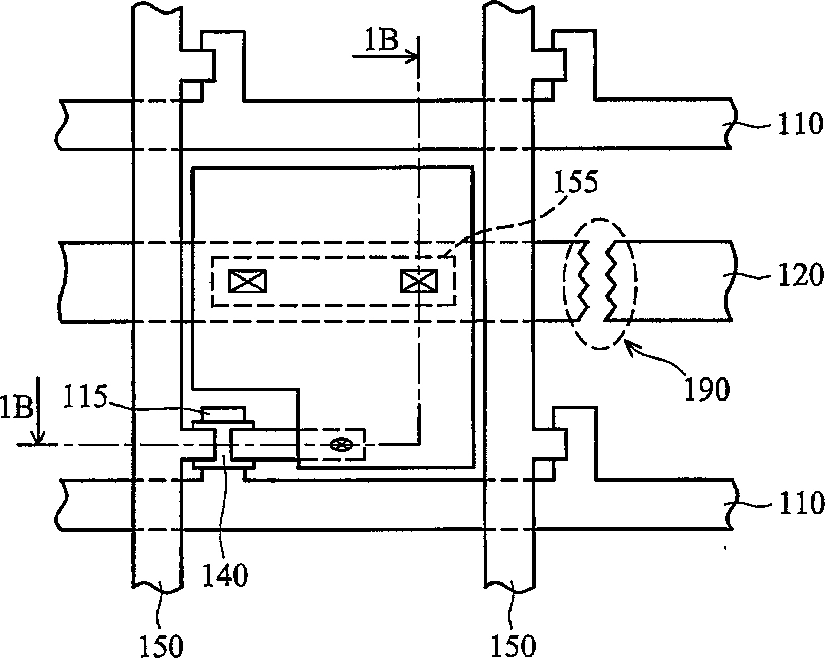
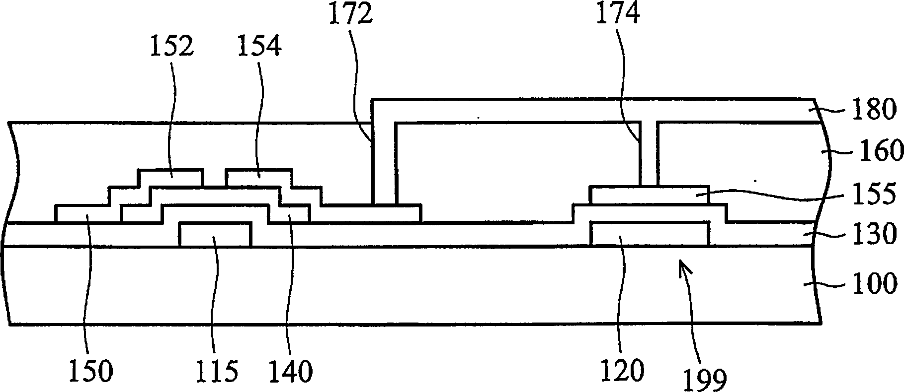
[0033] figure 2 is a partial plan view showing a liquid crystal display device according to a first embodiment of the present invention, and image 3 is along figure 2 The sectional view of line 3-3 in is used to illustrate the process of the first embodiment. It should be particularly noted here that although the following illustrations only show one pixel area, in fact the liquid crystal display device of the present invention may include many pixel areas.

[0034] see figure 2 and 3 , first provide an insulating substrate 200 (hereinafter referred to as a lower substrate) such as glass or quartz. A gate line 210 extending laterally and a discrete first metal layer 220 are formed on the lower substrate 200 , the gate line has a gate 215 . Wherein, the gate line 210 and the first metal layer 220 may be formed by the same deposition step, and the material thereof is, for example, Al, Cr, Mo or their alloys and other conductive materials.

[0035] Afterwards, a dielect...

no. 2 example

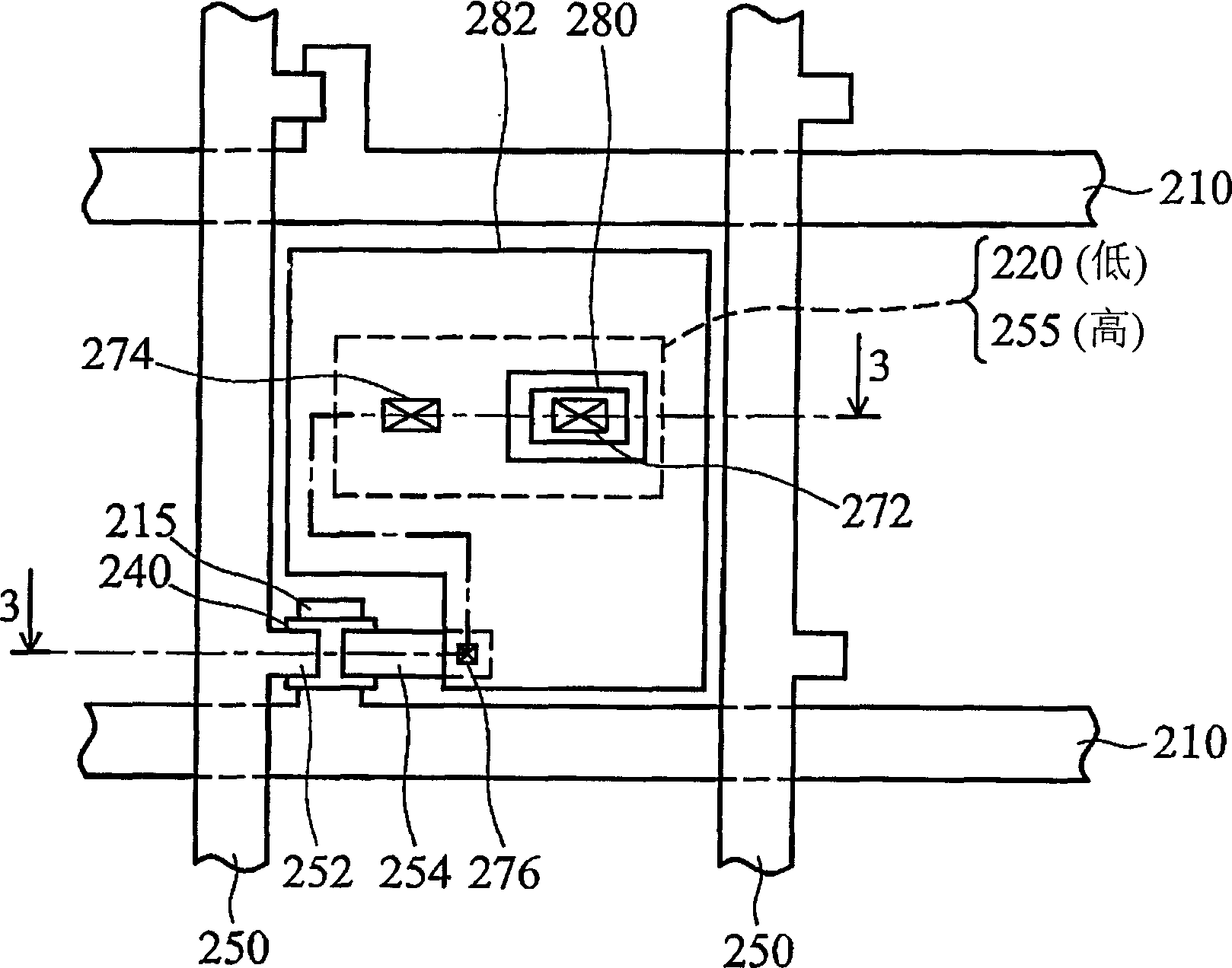
[0061] Figure 7 is a partial plan view showing a liquid crystal display device according to a second embodiment of the present invention, and Figure 8 is along Figure 7 The cross-sectional view of line 8-8 in the figure is used to illustrate the process of the second embodiment. It should be noted here that although the following diagrams only show one pixel area, in fact the liquid crystal display device of the present invention may include many pixel areas.

[0062] see Figure 7 and 8 , first provide an insulating substrate 700 (hereinafter referred to as a lower substrate) such as glass or quartz. A gate line 710 extending laterally and a separate layer of metal layer 720 are formed on the lower substrate 700 , the gate line has a gate 715 . Wherein, the gate line 710 and the metal layer 720 may be formed by the same deposition step, and the material thereof is, for example, a conductive material such as Al, Cr, Mo or an alloy thereof.

[0063] After that, a diele...


PUM


Abstract

It is a LCD device and its process method, which comprises the following steps: to form at least one storage capacitor structure composed of first metal layer, second metal layer and a dielectric layer in middle at the down base; then to form an isolation layer on the inner surface of the upper base and stretch it into the LCD layer to keep the thickness of the LCD layer; then to form a common electrode between the down base and the isolation layer, which are connected with the first metal layer though separately transparent conducting layer.

Description

technical field [0001] The present invention relates to a liquid crystal display device and a manufacturing method thereof, in particular to a liquid crystal display device without linear storage capacitor electrode lines (storage capacitance electrode lines, Cs-lines) and a manufacturing method thereof. Background technique [0002] A liquid crystal display device (LCD) includes an upper substrate and a lower substrate, and a liquid crystal layer sandwiched between the upper and lower substrates. Generally, the upper substrate has a color filter and a common electrode. The lower substrate has gate lines extending laterally, source lines (or data lines) extending vertically, thin film transistors (TFTs) serving as switching elements located near intersections of the gate lines and source lines, and A pixel electrode in an area defined by a gate line and a source line. Each thin film transistor has a gate, a source and a drain. The gate is extended from the gate line, and ...

Claims


Application Information

Patent Timeline
IPC IPC(8): G02F1/133G02F1/136H01L29/786
Inventor 张永吉
Owner AU OPTRONICS CORP
Why Eureka
Try Eureka