Digital application of protective soldermask to printed circuit boards

A technology of printed circuit board and solder mask, which is applied in the direction of printed circuit, printed circuit, printed circuit manufacturing, etc., can solve problems such as affecting steps, and achieve the effect of eliminating time-consuming

Inactive Publication Date: 2005-07-13
CAMTEK LTD
View PDF1 Cites 4 Cited by
  • Summary
  • Abstract
  • Description
  • Claims
  • Application Information

AI Technical Summary

Problems solved by technology

Step 150 may be affected using any conventional method, such as using "curtain coating" and "screen printing" methods.

Method used


Image

  • Digital application of protective soldermask to printed circuit boards
  • Digital application of protective soldermask to printed circuit boards
  • Digital application of protective soldermask to printed circuit boards

Examples


Embodiment Construction

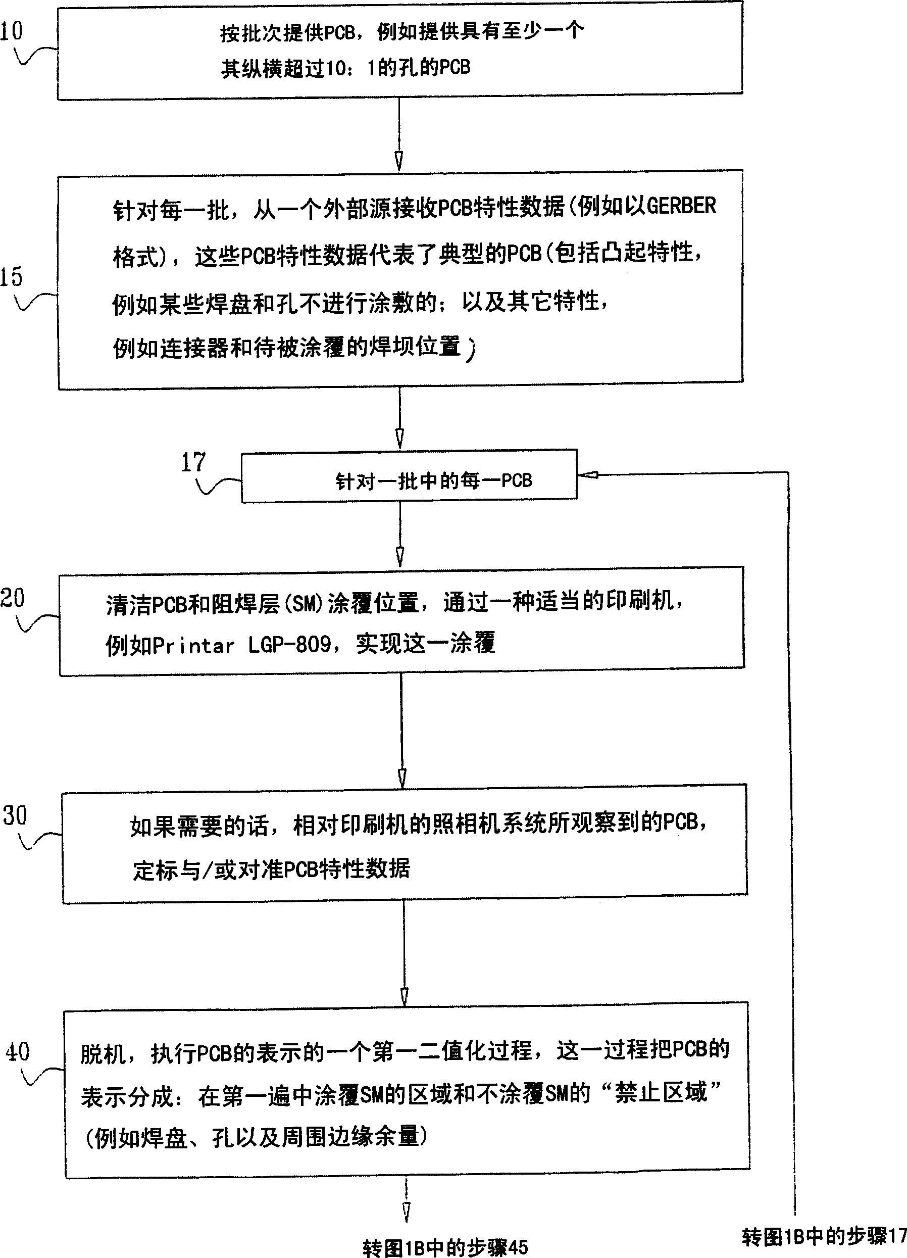
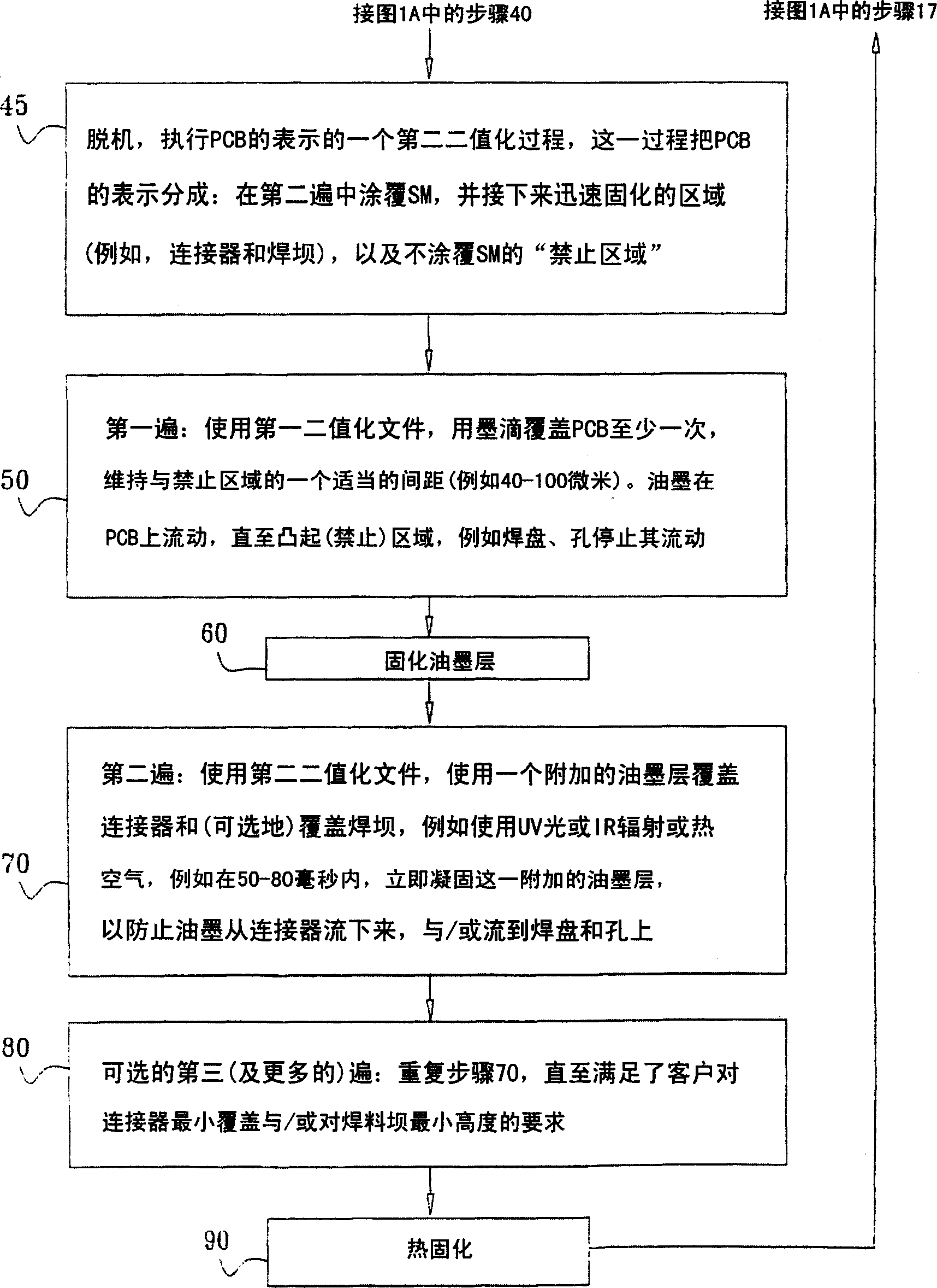
[0051] now refer to Figure 1A-1B . Figure 1A-1B Together, this forms a simplified flowchart of a method for digitally applying protective solder mask to a printed circuit board, constructed and operative in accordance with a preferred embodiment of the present invention.

[0052] Preferably, a digital solder resist drop placement system similar to that illustrated and described in published PCT application PCT / IL01 / 00596 (WO 02 / 01929) is used to achieve Figure 1A-1B Methods.

[0053] In step 50, drops of digital solder resist, also referred to herein as "ink drops", are placed over the entire area of ​​the circuit board except for the keep-out areas. These ink droplets flood the exposed parts of the printed circuit board. The copper layer has been etched away from these exposed parts, also referred to herein as the "lamination areas" of the printed circuit board. During the pouring process, the pad stops the flow of liquid solder mask. This step brings the solder mask clo...


PUM

PropertyMeasurementUnit
thicknessaaaaaaaaaa

Abstract

A method and apparatus for applying ink to a printed circuit board having raised pads defining pad edges according to a solder mask pattern. The method includes flooding the printed circuit board with ink such that the ink is able to advance to the edge of the pad and stop near or at the edge of the pad and does not climb onto the raised pad.

Description

technical field [0001] The present invention relates to an apparatus and method for applying a protective solder mask to a printed circuit board. Background technique [0002] In prior art Figure 2, a simplified flowchart illustration of a conventional method of applying a protective solder mask to a PCB (Printed Circuit Board) is depicted. Step 150 may be effected using any conventional method, such as using "curtain coating" and "screen printing" methods. [0003] Published PCT application WO 02 / 01929 A2 describes a jet printing based apparatus and method for the manufacture of printed circuit boards. [0004] All publications mentioned in this specification and the disclosures of publications cited therein are hereby incorporated by reference. Contents of the invention [0005] A common prior art method for applying solder mask on high-end printed circuit boards is photolithography, which involves the following steps: [0006] (a) pre-cleaning and washing circuit boa...

Claims


Application Information

Patent Timeline
Patent Type & Authority Applications(China)
IPC IPC(8): C08F2/48H05K3/00H05K3/28
CPCH05K3/0091H05K3/28H05K2201/09736H05K2201/09881H05K2203/013H05K2203/081H05K2203/1509
Inventor 罗恩·祖海尔雅各布·莫泽勒拉恩·威尔克
Owner CAMTEK LTD
Why Eureka
Try Eureka