Liquid crystal display apparatus and fabrication method of the same

A liquid crystal display and manufacturing method technology, which is applied in microlithography exposure equipment, chemical instruments and methods, semiconductor/solid-state device manufacturing, etc., can solve problems such as deterioration of pixel circuit performance and leakage current, and prevent orientation disorder and reduce costs. Reduced effect

Inactive Publication Date: 2005-07-20
NEC LCD TECH CORP
View PDF1 Cites 2 Cited by
  • Summary
  • Abstract
  • Description
  • Claims
  • Application Information

AI Technical Summary

Problems solved by technology

Therefore, another problem with this technology is that if the black matrix is ​​formed to cover the pixel circuit, there is a possibility of leakage current, so that the performance of the pixel circuit deteriorates

Method used


Image

  • Liquid crystal display apparatus and fabrication method of the same
  • Liquid crystal display apparatus and fabrication method of the same
  • Liquid crystal display apparatus and fabrication method of the same

Examples


Embodiment Construction

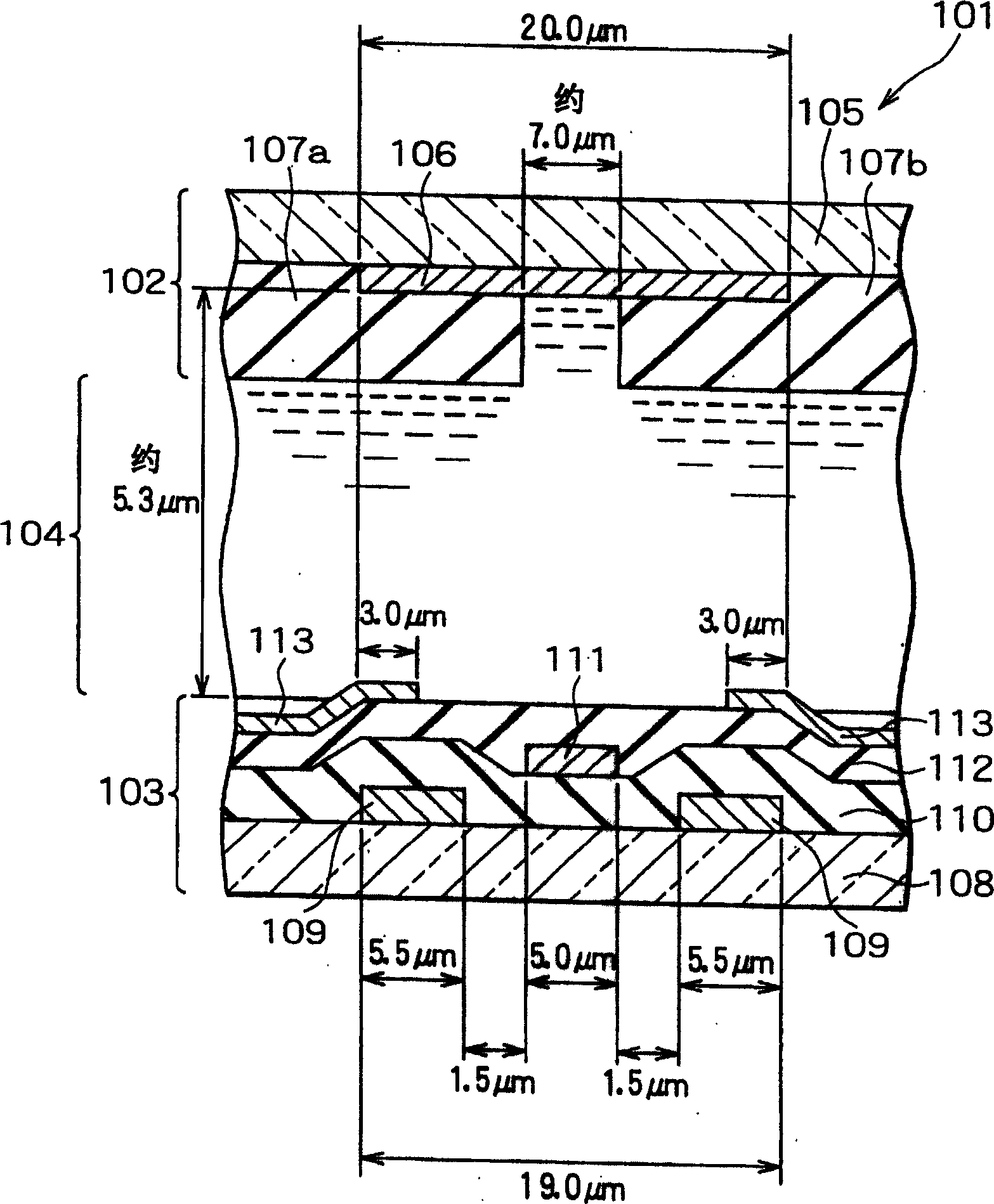
[0035] Embodiments of the present invention will be described below with reference to the drawings. Figure 5 is a sectional view showing a liquid crystal panel of a liquid crystal display device according to an embodiment of the present invention. The size of each part of the liquid crystal panel of this embodiment is Figure 5 shown as an example, but not limited to Figure 5 example shown. In the liquid crystal display device according to the present embodiment, a light source (not shown in the figure), a liquid crystal panel, and a frame body (not shown in the figure) accommodating these components are provided. Furthermore, if Figure 5 As shown, a liquid crystal panel 1 has a color filter substrate 2 and an array substrate 3 placed parallel to each other. A liquid crystal layer 4 is sealed between the color filter substrate 2 and the array substrate 3 .

[0036] In the color filter substrate 2 , there is provided a transparent substrate 5 formed of glass, for example, a...


PUM

PropertyMeasurementUnit
thicknessaaaaaaaaaa
angleaaaaaaaaaa
thicknessaaaaaaaaaa

Abstract

In a liquid crystal panel, a color filter substrate and an array substrate are provided in parallel with each other, and a liquid crystal layer is sealed therebetween. In the color filter substrate, a black matrix made of a resin and color filters are provided on a transparent substrate. In the array substrate, a pixel circuit is provided on a transparent substrate. The pixel circuit includes a gate interconnection, a gate insulating film, a semiconductor region, a drain interconnection, a passivation film, a pixel electrode, and the like. The sum of the step heights on the surfaces of the color filter substrate and the array substrate both facing the liquid crystal layer is 0.83 mum, and the pre-tilt angle of the liquid crystal layer is set to 4 degrees or more.

Description

technical field [0001] The present invention relates to a liquid crystal display device and a manufacturing method thereof. Background technique [0002] A liquid crystal display device has a light source and a liquid crystal panel. A liquid crystal panel has two transparent substrates and a liquid crystal layer filled between the transparent substrates. When a voltage is applied to the liquid crystal layer in the liquid crystal panel to control its light transmittance, the light source illuminates the liquid crystal panel, thereby displaying an image. To perform this operation, pixel circuits that apply voltage across the liquid crystal layer are located on one of the transparent substrates in the liquid crystal panel, and color filters are located on the other transparent substrate. The pixel circuit has, for example, a plurality of thin film transistors (TFTs) distributed in a matrix. In the following description, a substrate with pixel circuits is referred to as an "a...

Claims


Application Information

Patent Timeline
Patent Type & Authority Applications(China)
IPC IPC(8): G02B5/20G02F1/133G02F1/1333G02F1/1335G02F1/1337G02F1/136G02F1/1368G03F7/20H01L21/027
CPCG02F2001/136236G02F1/133512G02F2001/13373G02F1/13373G02F1/136236C02F1/4606C02F1/4618C02F1/505C02F2103/04
Inventor 冈本守
Owner NEC LCD TECH CORP
Why Eureka
Try Eureka