Electroluminescent device with a transparent cathode
An electroluminescence and equipment technology, applied in the field of electroluminescence equipment, can solve problems such as low light transmission rate
- Summary
- Abstract
- Description
- Claims
- Application Information
AI Technical Summary
Problems solved by technology
Method used
Image

Examples
Embodiment 1
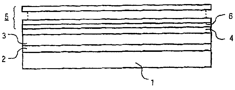
[0043] On a glass disk as substrate 1 a subsequently structured 140 nm thick ITO layer was provided as first electrode 2 . Next, a 200-nm-thick polyethylenedioxythiophene layer as a hole-guiding layer and an 80-nm-thick polymer (p-styrenevinylene) (PPV) layer as an electroluminescent layer 3 were successively provided. A second electrode 4 consisting of a 5 nm thick barium layer and a 15 nm thick aluminum layer is provided on this PPV layer. A 43nm thick ZnS layer was deposited on the aluminum layer.
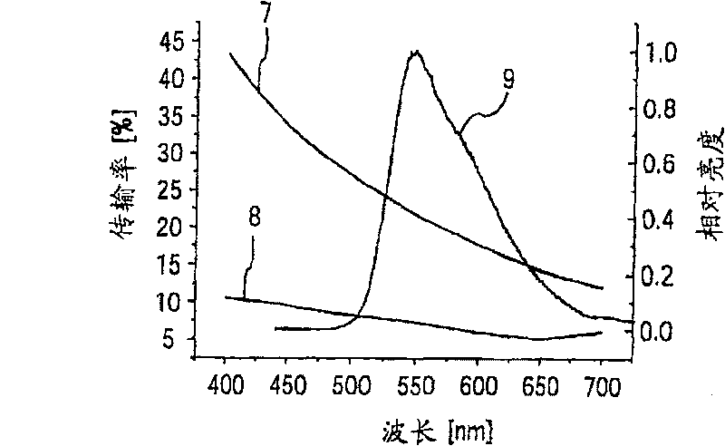
[0044] image 3 The transmission characteristics of the second electrode are shown in curve 11 of . With uncoated electrodes ( figure 2 Compared with curve 8) in , the transmission rate of the light generated in the electroluminescent layer 3 through the second electrode can be increased. In addition, the transmission rate in the blue spectral region is reduced.
Embodiment 2
[0046] An electroluminescent device similar to that in Example 1 was fabricated except that the second electrode contained a 25 nm thick layer of silver instead of the aluminum layer, and the thickness of ZnS was 38 nm.
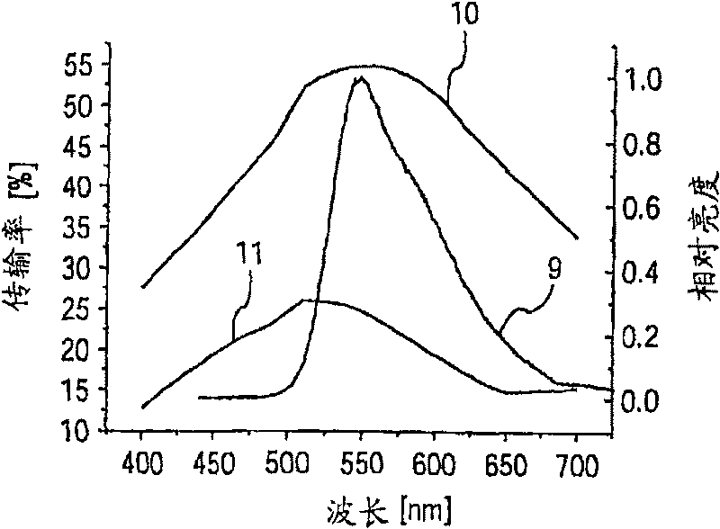
[0047] image 3 The curve 10 of the graph shows the transmission rate of the light emitted by the electroluminescent layer 3 on the second electrode 4 . With uncoated electrodes ( figure 2 Compared to curve 7) in , the transfer rate can be increased. In addition, the filter effect in the blue and red spectral regions is maintained.
Embodiment 3
[0049] An electroluminescence device similar to that described in Example 2 was fabricated except that three transparent insulating layers 5 were stacked on the second electrode 4 . The thickness of the first transparent insulating ZnS layer adjacent to the second electrode 4 is 41nm, and the second transparent insulating MgF 2 The layer thickness is 84 nm, while the third transparent insulating ZnS layer has a thickness of 55 nm.
[0050] Figure 4 The transmission characteristic of the second electrode 4 is shown in the curve 12 of . with a single covered electrode ( image 3 Compared with the middle curve 10), this transmission characteristic can be adapted to the emission spectrum of the PPV electroluminescent layer (cf. Figure 4 Middle curve 9).
PUM
| Property | Measurement | Unit |
|---|---|---|
| thickness | aaaaa | aaaaa |
| refractive index | aaaaa | aaaaa |
Abstract
Description
Claims
Application Information
 - R&D
- Intellectual Property
- Life Sciences
- Materials
- Tech Scout
- Unparalleled Data Quality
- Higher Quality Content
- 60% Fewer Hallucinations
Browse by: Latest US Patents, China's latest patents, Technical Efficacy Thesaurus, Application Domain, Technology Topic, Popular Technical Reports.
© 2025 PatSnap. All rights reserved.Legal|Privacy policy|Modern Slavery Act Transparency Statement|Sitemap|About US| Contact US: help@patsnap.com