Method for realizing silicon based silicon dioxde waveguide polarization irrelevancy by employing non-planar process

A silicon dioxide, non-planar technology, used in optical waveguides, light guides, optics, etc., to solve problems such as polarization insensitivity

Inactive Publication Date: 2005-09-21
INST OF SEMICONDUCTORS - CHINESE ACAD OF SCI
View PDF0 Cites 14 Cited by
  • Summary
  • Abstract
  • Description
  • Claims
  • Application Information

AI Technical Summary

Problems solved by technology

The realization of polarization insensitivity of waveguides and related devices has not been reported internationally

Method used


Image

  • Method for realizing silicon based silicon dioxde waveguide polarization irrelevancy by employing non-planar process
  • Method for realizing silicon based silicon dioxde waveguide polarization irrelevancy by employing non-planar process
  • Method for realizing silicon based silicon dioxde waveguide polarization irrelevancy by employing non-planar process

Examples


Embodiment Construction

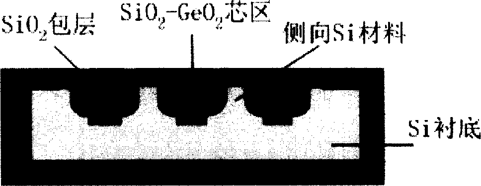
[0022] see image 3 , Figure 3-1 , image 3 -2 is to perform reactive ion etching (RIE) on the silicon substrate 11 first, etch out the square waveguide core space 12, the space width is 22.8 μm, the etching depth is not less than 21 μm, and the core space spacing is not less than 30 μm ; Figure 3-3 A lower cladding layer and lateral cladding layer 13 with a thickness of about 15 μm are formed by high-temperature thermal oxidation to limit light leakage; Figure 3-4 The core region 14 is grown by plasma enhanced chemical vapor deposition (PECVD) or flame hydrolysis (FHD) in the core space of the waveguide, the thickness of the core layer is controlled to 6 μm, and the refractive index is 0.75 according to the difference between the refractive index of the core region and the cladding layer. % to determine, the core material can be P 2 o 5 -GeO 2 -SiO 2 、GeO 2 -SiO 2 , SiON or P 2 o 5 -SiO 2 ; image 3 -5 is to use the FHD method or the PECVD method to grow the u...


PUM


Abstract

This invention relates to a silicon base dioxide silicon wave polarization switch method by use of non-plane process and is characterized by the following steps: a, etching the ion on the silicon underlay for wave guide core area space; b, forming down cover layer and side cover layer with thickness of 15 mu m; c, growing core area by use of ion strengthening chemical gas deposition method and flame solution in wave guide core area; d, growing upper cover layer of 15 mu m by use of ion strengthening chemical gas deposition method or flame solution; f, polishing and removing the core layer of the oxidation layer, upper cover of materials; whole silicon dioxide silicon polarization wave guide process.

Description

technical field [0001] The invention relates to silicon-based silicon dioxide stress optical waveguide devices, which are used to realize the polarization insensitivity of this type of waveguide, in particular to silicon-based silicon dioxide arrayed waveguide gratings (AWG), optical switches and Mach-Zehnder interference ( MZI) type devices are not polarization sensitive. Background technique [0002] Silicon-based silica optical waveguide is an optical waveguide formed by depositing silicon dioxide on a silicon substrate first and then etching. Because the thermal expansion coefficients of silicon dioxide and silicon substrate are inconsistent, the prepared waveguide has stress asymmetry. The optical waveguide exhibits a large stress birefringence with a birefringence index of about 10 -4 order of magnitude, and general devices are required to be insensitive to polarization, and the birefringence index of the entire waveguide needs to be reduced to 10 -5 Therefore, reali...

Claims


Application Information

Patent Timeline
Patent Type & Authority Applications(China)
IPC IPC(8): G02B6/10G02B6/136
Inventor 安俊明李健郜定山夏君磊李建光王红杰胡雄伟
Owner INST OF SEMICONDUCTORS - CHINESE ACAD OF SCI
Why Eureka
Try Eureka