Method for realizing stress optical waveguide polarization insensitivity of silicon group silicon dioxide with symmetric structure

A symmetrical structure, silicon dioxide technology, applied in the direction of optical waveguide and light guide, which can solve the problem of insensitivity to polarization of waveguides and related devices

Inactive Publication Date: 2005-11-09
INST OF SEMICONDUCTORS - CHINESE ACAD OF SCI
View PDF0 Cites 0 Cited by
  • Summary
  • Abstract
  • Description
  • Claims
  • Application Information

AI Technical Summary

Problems solved by technology

However, using PECVD to grow a high-refractive-index SiON compensation layer that can adjust the birefringence coefficient of the waveguide, half of the compensation layer is etched symmetrically in the center of the waveguide to achieve polarization insensitivity of the waveguide and related devices has not been reported internationally.

Method used


Image

  • Method for realizing stress optical waveguide polarization insensitivity of silicon group silicon dioxide with symmetric structure
  • Method for realizing stress optical waveguide polarization insensitivity of silicon group silicon dioxide with symmetric structure
  • Method for realizing stress optical waveguide polarization insensitivity of silicon group silicon dioxide with symmetric structure

Examples


Embodiment Construction

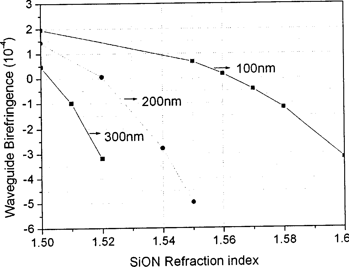
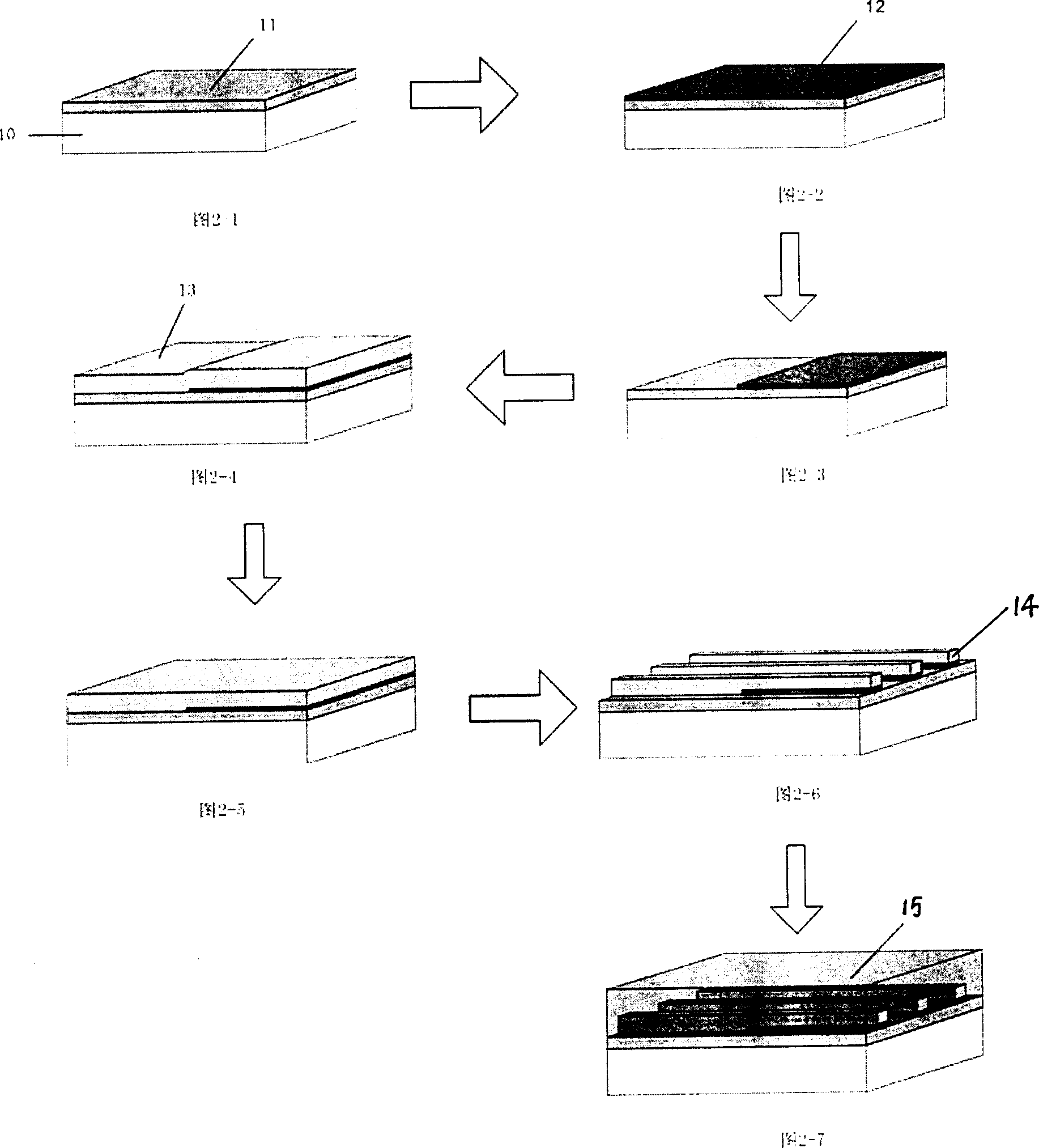
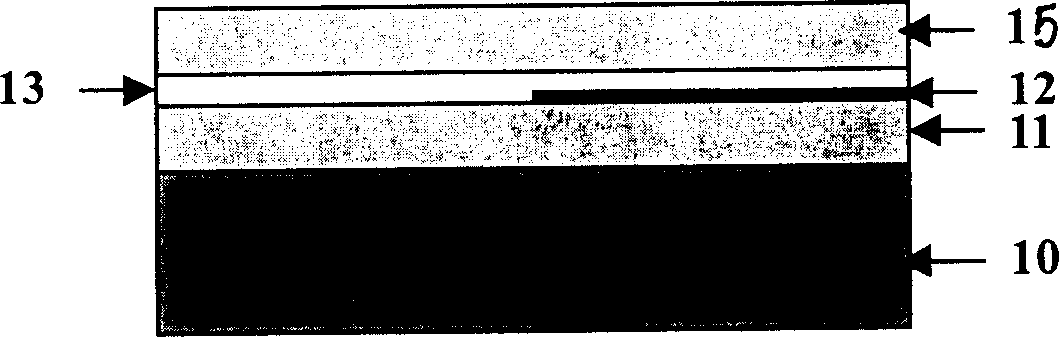
[0031] see figure 2 , diagram 2-1 On the silicon substrate 10, use thermal oxidation, flame hydrolysis (FHD) or plasma enhanced chemical vapor deposition (PECVD) to form a silicon dioxide lower cladding layer 11 with a thickness of not less than 15 μm to limit light leakage ; Figure 2-2 The high refractive index SiON compensation layer 12 with adjustable waveguide birefringence is grown by PECVD method. The thickness and refractive index of the SiON compensation layer should be adjusted according to the birefringence of the actual silicon-based silicon dioxide stress optical waveguide. The refractive index can be adjusted by Control the content of N to achieve; Figure 2-3 Half of the SiON compensation layer 12 is symmetrically etched away by reactive ion etching (RCE) at the waveguide symmetry center; Figure 2-4 The core layer 13 with a thickness of 6 μm is grown by FHD method or PECVD method, and the refractive index is determined according to the refractive index dif...


PUM


Abstract

A method for realizing the polarization-insensitive silicon-based silica stress optical waveguide having a symmetrical structure, comprising the steps of: (1) using thermal oxidation, flame hydrolysis or plasma enhanced chemical vapor deposition on a silicon substrate Form the lower cladding layer of silicon dioxide; (2) use plasma-enhanced chemical vapor deposition to grow a high-refractive-index SiON compensation layer that can adjust the birefringence index of the waveguide; (3) symmetrically etch away the center of the waveguide with reactive ion etching half; (4) growing the core layer by flame hydrolysis or plasma enhanced chemical vapor deposition; (5) polishing; (6) etching the core layer by reactive ion etching to form an optical waveguide layer with a strip-like symmetrical structure; (7) The upper cladding is grown by the flame hydrolysis method or the plasma enhanced chemical vapor deposition method, and the silicon-based silicon dioxide polarization-insensitive stress optical waveguide with the entire symmetrical structure is prepared.

Description

technical field [0001] The present invention relates to silicon-based silicon dioxide stress optical waveguide devices with a symmetrical structure, used to realize the polarization insensitivity of this type of waveguide, especially silicon-based silicon dioxide arrayed waveguide grating (AWG) and Mach-Zehnder interference (MZI) type devices are not polarization sensitive. Background technique [0002] Silicon-based silica optical waveguide is an optical waveguide formed by depositing silicon dioxide on a silicon substrate and etching it. Because the thermal expansion coefficients of silicon dioxide and silicon substrate are inconsistent, the prepared waveguide has stress asymmetry. The waveguide exhibits large stress birefringence with a birefringence index of about 10 -4 order of magnitude, and general devices are required to be insensitive to polarization, and the birefringence index of the entire waveguide needs to be reduced to 10 -5 Therefore, realizing the polariza...

Claims


Application Information

Patent Timeline
Patent Type & Authority Patents(China)
IPC IPC(8): G02B6/13
Inventor 安俊明李健郜定山夏君磊李建光王红杰胡雄伟
Owner INST OF SEMICONDUCTORS - CHINESE ACAD OF SCI
Why Eureka
Try Eureka