Surface texture structure and a minimized and localized lattice constant and thermal expansion factor mismatching method
A surface texture and device technology, applied in the field of semiconductor optoelectronics, can solve the problems of lack of mismatch effects and other problems
- Summary
- Abstract
- Description
- Claims
- Application Information
AI Technical Summary
Problems solved by technology
Method used
Image
Examples
example
[0032] (1) The epitaxial layer in the present invention includes, but not limited to, an N-type confinement layer, a P-type confinement layer, and a light-emitting layer;
[0033] (2) The growth substrate in the present invention includes a luminescent growth substrate and a non-luminescent growth substrate;
[0034] (3) The "buffer layer" of the present invention includes a single-layer buffer layer and a multi-layer buffer layer.
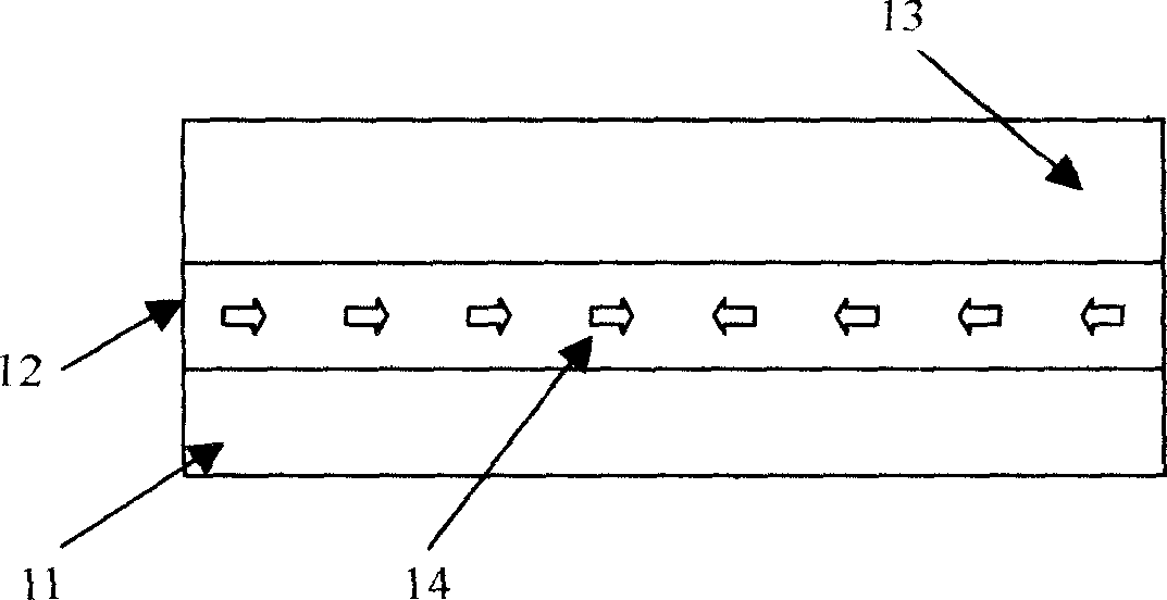
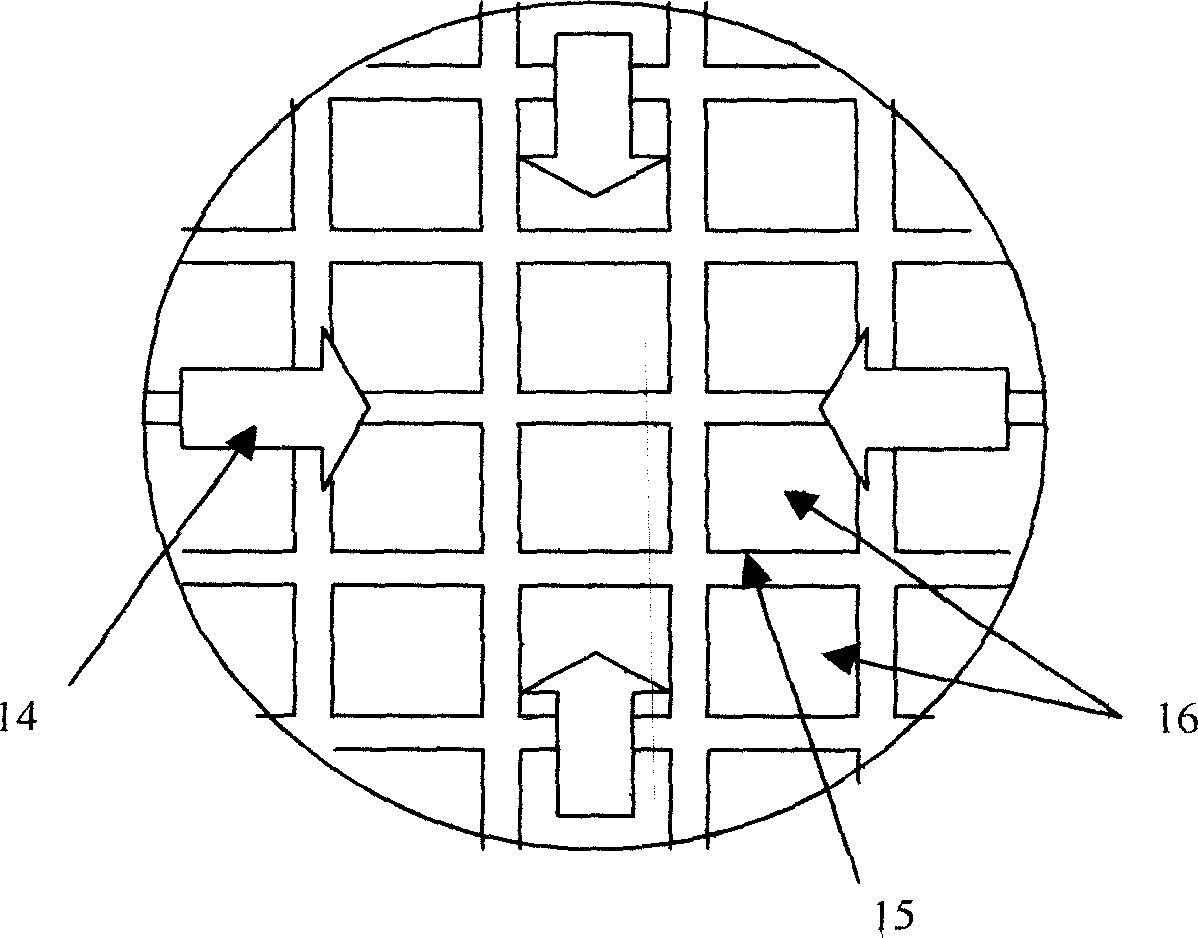
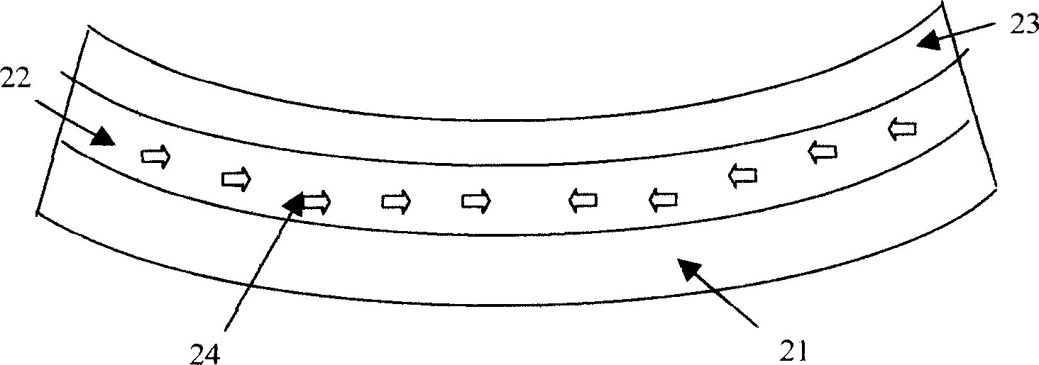
[0035] Figure 1a shows a cross-sectional view of a previous thicker growth substrate and the epitaxial layer thereon. The buffer layer 12 is grown on the upper surface of the growth substrate 11 , and the epitaxial layer 13 is grown on the upper surface of the buffer layer 12 . A force 14 generated by the mismatch of the lattice constant and the thermal expansion coefficient exists at and parallel to the interface between the buffer layer 12 and the growth substrate 11 . Before grinding thinning, the growth substrate 11 is sufficiently thick tha...
PUM
 Abstract
Description
Claims
Application Information


