Non-volatile memory circuit and semiconductor device

A non-volatile storage and circuit technology, which is applied in the manufacture of semiconductor devices, circuits, semiconductor/solid-state devices, etc., can solve the problems of increased circuit size, increased chip size, and increased manufacturing costs, and achieve reduced manufacturing costs. The effect of solving cost and inventory problems

Inactive Publication Date: 2005-10-05
SEIKO INSTR INC
View PDF1 Cites 6 Cited by
  • Summary
  • Abstract
  • Description
  • Claims
  • Application Information

AI Technical Summary

Problems solved by technology

However, this leads to an increase in circuit size and thus chip size
This also results in increased manufacturing costs and cannot be mounted in currently available packages

Method used


Image

  • Non-volatile memory circuit and semiconductor device
  • Non-volatile memory circuit and semiconductor device
  • Non-volatile memory circuit and semiconductor device

Examples


Embodiment 1

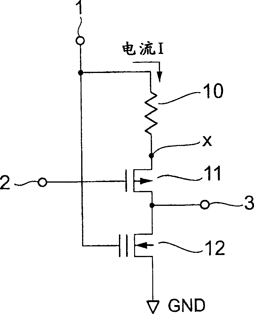
[0024] figure 1 The EPROM read / write circuit according to the present invention is shown. The resistor 10, the PMOS transistor 11, and the EPROM 12 are connected in series with each other between the power supply voltage terminal 1 and the GND terminal. The gate of the PMOS transistor 11 is connected to the write control terminal 2 and the gate of the EPROM 12 is connected to the power supply voltage terminal 1.

[0025] In order to perform writing to the EPROM 12, an optimum voltage difference for writing is required between the gate terminal and the drain terminal of the EPROM 12. Therefore, the voltage Vw that is most suitable for writing in terms of EPROM 12 characteristics is applied to the power supply voltage terminal 1.

[0026] In addition, when the PMOS transistor 11 is in an on state, a current I [A] flows between the source and drain of the EPROM. The resistor 10 sets an optimal voltage value at which the current is injected into the floating gate of the EPROM 12. Wh...

Embodiment 2

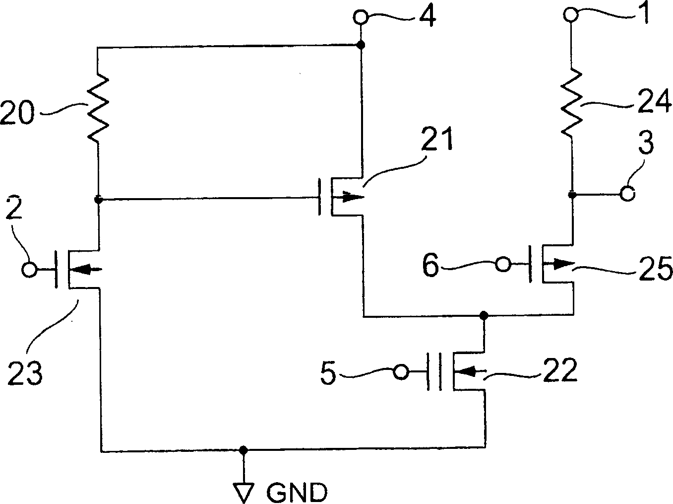
[0035] Figure 5 It is a circuit diagram of the EPROM read / write circuit of the present invention for the trimming circuit. Figure 5 The trimming circuit in is composed of a storage circuit 50 and a voltage divider resistor network 51. The voltage dividing resistor network 51 is composed of resistors and MOS switches connected to both ends of these resistors. The storage circuit 50 includes figure 1 The number of EPROM read / write circuits shown corresponds to the number of resistors constituting the voltage divider resistor network 51. The gate terminal of each MOS switch is connected to figure 1 The EPROM read / write circuit in the output voltage terminal 3 is connected. The voltage Vr is applied to the power supply voltage terminal, and the potential of Vr is the same as when the EPROM is read.

[0036] The data output of the storage circuit corresponding to the storage state of the EPROM is supplied to the gate of each MOS switch, thereby performing on / off control of the MOS ...


PUM


Abstract

The invention executes writing / reading in / from an EPROM without adding any signal terminal by generating an EPROM writing voltage by resistance in a trimming circuit having the EPROM. When writing to the EPROM is executed, a drop voltage by resistance is set as a writing voltage by a power supply voltage terminal. Thus, the writing / reading in / from the EPROM is executed without disposing any writing terminal.

Description

Technical field [0001] The present invention relates to an electrically writable nonvolatile memory circuit, and a semiconductor device having a trimming device using the circuit. Background technique [0002] In recent years, a large number of power control ICs have been combined and used in various electronic products. The setting voltage of the power control IC is not only different, but also accurately set according to its application before packaging it in the manufacturing plant. Therefore, in addition to the high manufacturing cost of power control ICs, the electronic equipment industry also encounters inventory problems. [0003] In view of the above problems, there is a need for a power control IC in which the required voltage can be set after packaging, and the power control IC can solve the problem of high manufacturing cost and inventory problems. Therefore, a power control IC with an electrically writable nonvolatile memory circuit is proposed. [0004] Figure 2 show...

Claims


Application Information

Patent Timeline
Patent Type & Authority Applications(China)
IPC IPC(8): G11C16/06G11C16/12G11C16/26G11C29/02H01L21/8247H01L27/115H01L29/788H01L29/792
CPCG11C29/021G11C16/04G11C16/12G11C29/02G11C29/028G11C2029/5004H01L21/822
Inventor 酒井雅司出口充康
Owner SEIKO INSTR INC
Why Eureka
Try Eureka