

Integrated plating and planarization process and apparatus therefor
A planarization, equipment technology, used in the field of semiconductor processing
- Summary
- Abstract
- Description
- Claims
- Application Information
AI Technical Summary
Problems solved by technology
Method used
Image

Examples
Embodiment Construction
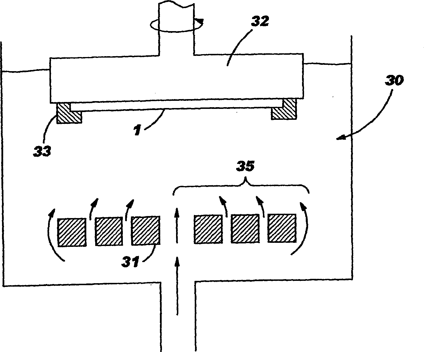
[0026] According to the present invention, an apparatus is provided that allows CMP to be performed after metal deposition (electroplating) and metal removal (electroetching) in optional steps, where each step has discrete process conditions and does not require Remove the wafer from the device. Copper plating and removal will be described to illustrate the invention. It should be understood that the present invention is not limited to the type of material deposited on the wafer.
[0027] Embodiments of the present invention may be understood as modifications of CMP equipment. A conventional CMP apparatus is schematically shown in Fig. ID. Wafer 1 is fixed upwards on wafer carrier 12 which rotates relative to table 10 with polishing pad 20 and polishing slurry thereon. The polishing rate is determined in part by the force with which the wafer 1 is pressed against the polishing pad 20 . Thus, the wafer carrier 12 is adjustable to provide a variable force on the polishing pa...
PUM
 Abstract
Description
Claims
Application Information