Process for producing electrophoresis display device

A manufacturing method and electro-display technology, which can be applied to instruments, nonlinear optics, optics, etc., can solve the problems of uniformly setting sealing materials, narrowing the selection range of sealing film materials, and limiting the specific gravity of sealing materials, and achieve the effect of good adhesion.

Inactive Publication Date: 2005-12-07
CANON KK
2 Cites 26 Cited by

AI-Extracted Technical Summary

Problems solved by technology

[0008] Second, there is a problem that the specific gravity of the sealing material is limited, thereby narrowing the selection range of sealing membrane materials
[0009] Third, there is a problem that ...

Method used

In this step, by polymerization, at least the polymerizable compound that constitutes the adhesive film matrix layer and the polymerizable compound that constitutes the sealing film matrix that are arranged at the upper end of the partition wall are bonded to each other, thereby strengthening the bond between the sealing film and the adhesive film. Adhesion between. On the other hand, the adhesive film is bonded to the upper end portion of the partition wall as described above. Therefore, the adhesiveness of the sealing film prepared in this step to the partition wall can be ensured.
[0119] The polymerizable compound preferably has an affinity for the partition wall. This is because not only disposing the polymerizable compound at the upper end portion of the partition wall is easy to perform, but also because the adhesiveness between the polymer of the polymerizable compound and the partition wall is good after polymerization of the polymerizable compound.
[0120] When necessary, treatment may be performed to enhance the adhesiveness of the polymer of the polymerizable compound provided at least at the upper end of the partition wall to the upper end of the partition wall. Adhesiveness is improved by, for example, forming minute unevenness at the upper end of the partition wall by, for example, dry etching. Alternatively, the polymerizable compound may be chemically fixed to at least the upper end of the partition wall using a functional group (such as -OH or -COOH) formed by subjecting at least the upper end of the partition wall to ozone treatment. ...

Abstract

An electric display device of the type wherein a dispersion liquid (40) comprising at least a dispersion medium and electrophoretic particles (50) is disposed in a space defined by a substrate (10), a partition wall (20) disposed on the substrate, and a sealing film (30) disposed on an upper end portion (90) of the partition wall is produced through a process including a step of disposing a sealing film precursor (120), comprising a polymerizable compound, supported by a supporting member (130) on both an exposed surface of the dispersion liquid and at least a part of the upper end portion (90) of the partition wall (20) in a state that the dispersion liquid is filled between adjacent partition walls, and a step of polymerizing the polymerizable compound to form the sealing film (30).

Application Domain

Non-linear optics

Technology Topic

Chemical compoundEngineering +2

Image

  • Process for producing electrophoresis display device
  • Process for producing electrophoresis display device
  • Process for producing electrophoresis display device

Examples

  • Experimental program(22)

Example Embodiment

[0164] Example 1
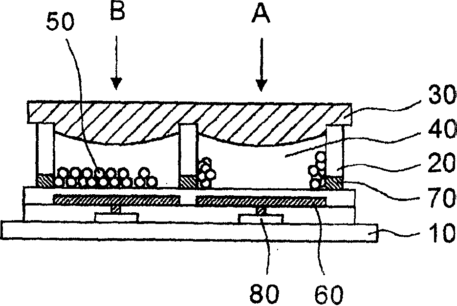
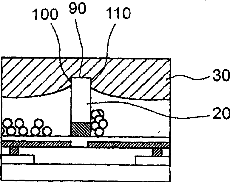
[0165] preparation figure 1 The electric display device shown in.
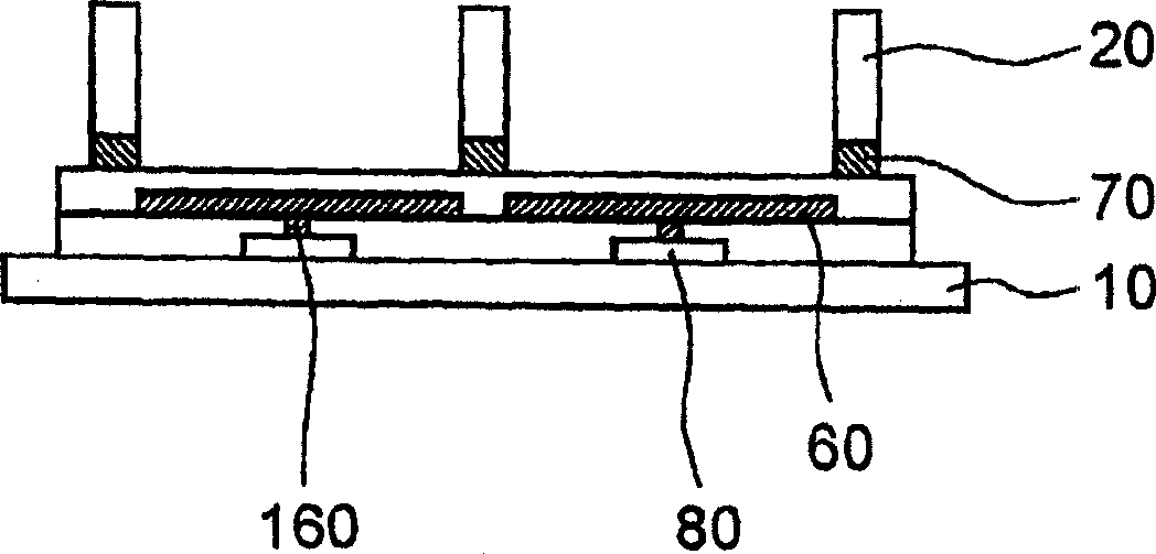
[0166]The resulting display device has 200×600 pixels, and each pixel has a size of 240 μm×80 μm. Each pixel is surrounded by a partition wall 20 having a width of 8 μm and a height of 28 μm. The first electrode 60 is provided between adjacent partition walls 20 and is connected to the switch device 80. The second electrode 70 is provided between the partition wall 20 and the substrate 10. The second electrode 70 is an electrode common to all pixels.
[0167] Will refer to image 3 -5 and 10 describe the specific manufacturing method of the display device in this embodiment.
[0168] The switching device 80 is formed on a stainless steel substrate 10 having a thickness of 0.1 mm. The substrate is then coated with an acrylic resin insulating layer, and the insulating layer is provided with contact holes. After that, on the insulating layer, a resist pattern for scattering incident light is formed, and an aluminum first electrode 60 is formed on the resist pattern, and the first electrode 60 is connected to the switch provided on the substrate 10 through the contact hole. The device 80 is electrically connected. The first electrode 60 is covered with an acrylic resin layer. In this example, the first electrode 60 also serves as a light reflection/scattering layer ( image 3 ). On the acrylic resin layer, a deep black titanium carbide second electrode 70 and a partition wall 20 of a pure photoresist product ("SU-8" manufactured by 3M Company) are formed in a thick film by a known photolithography method. After the second electrode 70 is formed, the surface of the acrylic resin layer on the first electrode 60 and the surface of the second electrode 70 are covered with a polycarbonate layer.
[0169] After coating, each pixel is filled with a dispersion liquid containing a dispersion medium 40 and electrophoretic particles 50 (FIG. 10 ). Isoparaffin (trade name: “Isoper H”; specific gravity: 0.76; manufactured by Exxon Corporation) can be used as the dispersion medium 40. As the electrophoretic compound 50, particles (average particle size: 1-2 μm) of styrene-methyl methacrylate copolymer resin containing carbon black are used. In the isoparaffin, succinimide (trade name: "OLOA1200", manufactured by Shevron Corporation) is added as a charge control agent.
[0170] On the other hand, the sealing film mother layer 120 is formed on the PET substrate as the supporting member 130 (FIG. 10). 1,4-Butanediol diglycidyl ether diacrylate (trade name: "NK oligo EA-5520"; specific gravity: not less than 1; manufactured by Shin Nakamura Kagaku Kogyo KK) as a UV curable monomer can be used as Sealing film matrix. This acrylate monomer and Isoper H (as a dispersion medium) are incompatible with each other, and the specific gravity of the acrylate monomer is greater than that of Isoper H.
[0171] On the support element 130 prepared above, an acrylate monomer mixed with 5 wt% of a photopolymerization initiator ("Irgacure 184" available from Ciba-Gaigy Co., Ltd.) was spin-coated to form a sealing film precursor with a thickness of 7 μm层120.
[0172] After that, the supporting member 130 is placed on the partition wall 20 and the dispersion medium 40, and the sealing film precursor layer 120 is brought into contact with the partition wall 20 and the dispersion medium 40 (FIG. 10). After contacting for a few seconds, the sealing film precursor layer 120 pushes the dispersion away so that it does not contact the partition wall 20, and finally the sealing film precursor layer 120 covers the upper end of the partition wall 20 and the exposed (outer) surface of the dispersion liquid. State ( Figure 4 ).
[0173] After this state is produced, the structure produced at room temperature is irradiated with UV light with an intensity of 0.3 mW/cm for 5 minutes, causing the sealing film precursor to polymerize. As a result, a cured sealing film 30 is formed (FIG. 5).
[0174] After the polymerization, when the resulting display device was viewed from the side close to the sealing film 30, no electrophoretic particles 50 were observed at the upper end of the partition wall 20 and inside the sealing film 30. In other words, during the polymerization process, the electrophoretic particles 50 are not included in the sealing film 30.
[0175] Then, by alternately adjusting the potential of the second electrode at a frequency of 1 Hz between +15V and -15V, while grounding the first electrode, the display device of this example was driven. As a result, while the alternating potential is adjusted, the resulting display state alternately changes between the black state and the white state.
[0176] Even if the display device continues to be driven, a phenomenon that the electrophoretic particles 50 move to overflow the partition wall 20 is not observed. In other words, it was confirmed that the dispersion liquid was restricted by the sealing film, the partition wall, and the substrate. It was also confirmed that the sealing film adhered to the partition wall without peeling.

Example Embodiment

[0177] Example 2
[0178] Except for removing the support member 130 from the sealing film 30 and exposing the sealing film 30 to the surrounding air, an electric display device was prepared in the same manner as in Example 1.
[0179] When the display device is driven in the same manner as in Embodiment 1, the display device exhibits the same display state change as in Embodiment 1. When the display device was driven, no phenomenon in which the electrophoretic particles 50 moved to overflow the partition wall 20 was observed. In addition, peeling of the sealing film 30 from the side of the partition wall 20 and volatilization of the dispersion medium 40 were not observed, which proved that the sealing film 30 and the partition wall 20 were adhered to each other.
[0180] Thus, even though the display device is bent backward and forward, no phenomenon is observed that the electrophoretic particles 50 move so as to overflow the partition wall. In addition, in the state where the display device was bent or bent inward, the driving of the display device was evaluated in the same manner as in Example 1. As a result, the same display state change as in Example 1 was observed.

Example Embodiment

[0181] Example 3
[0182] An electric display device was prepared in the same manner as in Example 1, except that the sealing film precursor was changed to polyethylene glycol methacrylate (trade name: "PE200"; specific gravity: not less than 1; manufactured by Nippon Yushi K.K.). Methacrylate is insoluble in Isoper H, and its specific gravity is greater than that of Isoper H.
[0183] When the resulting display device was driven the same as in Example 1, the same display state change as in Example 1 was observed. Even if the display device is continuously driven, no phenomenon that the electrophoretic particles 50 move so as to overflow the partition wall 20 is not observed. In addition, the sealing film 30 did not peel off from the partition wall side.

PUM

PropertyMeasurementUnit
Aperture50.0µm
Height5.0µm
Thickness7.0µm

Description & Claims & Application Information

We can also present the details of the Description, Claims and Application information to help users get a comprehensive understanding of the technical details of the patent, such as background art, summary of invention, brief description of drawings, description of embodiments, and other original content. On the other hand, users can also determine the specific scope of protection of the technology through the list of claims; as well as understand the changes in the life cycle of the technology with the presentation of the patent timeline. Login to view more.

Similar technology patents

Flexographic printing process with wet on wet capability

InactiveUS20110247508A1high color strengthgood adhesion
Owner:TECHNOSOLUTIONS ASSESSORIA

Foam double-sided tape and preparation method and application thereof

ActiveCN110003814AGood adhesionGood resistance to curved surface and anti-warping
Owner:安徽屹珹新材料科技有限公司

Classification and recommendation of technical efficacy words

  • good adhesion

Devices having a textured surface

ActiveUS7645475B2good adhesionreduce capsular contraction
Owner:MENTOR WORLDWIDE

Method for preparing hyperbranched polyester modified organic silicon resin

ActiveCN102504271AGood acid resistance and salt spray resistancegood adhesion
Owner:HANGZHOU JIHUA POLYMER MATERIAL CO LTD

Photovoltaic modules with polypropylene based backsheet

ActiveUS20120111407A1good adhesiongood extrusion
Owner:XIAN YUANFAR INT TRADE CO

Acid alcohol resin for light-smell dope and preparation method of acid alcohol resin

ActiveCN103435791Agood adhesionGood leveling
Owner:山东奔腾漆业股份有限公司
Why Eureka
Try Eureka