Electrostatic chuck wafer port and top plate with edge shielding and gas scavenging
An electrostatic chuck and wafer technology, applied in circuits, electrical components, gaseous chemical plating, etc., can solve problems such as the deterioration of edge cooling problems, failure to provide wafer mechanical devices, etc.
- Summary
- Abstract
- Description
- Claims
- Application Information
AI Technical Summary
Problems solved by technology
Method used
Image

Examples
Embodiment Construction
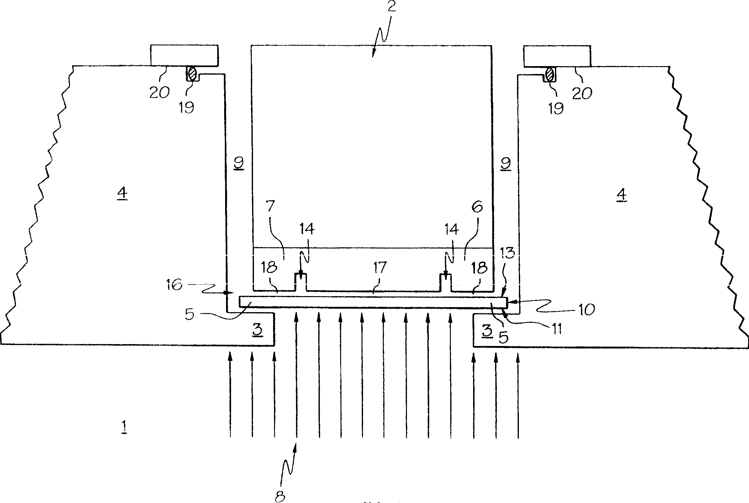
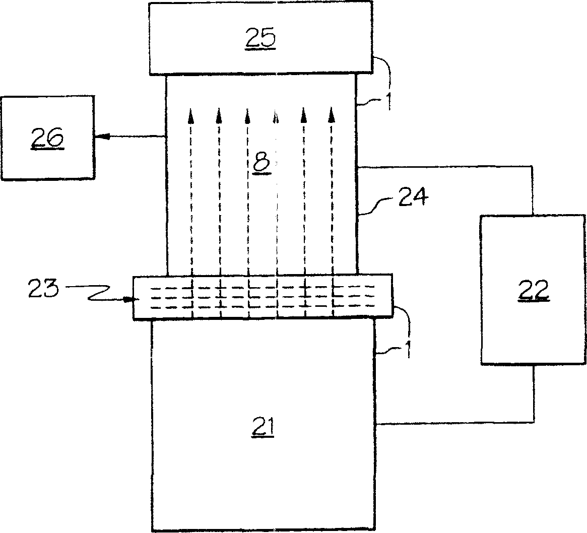
[0015] first reference figure 1 , illustrates an apparatus for processing a semiconductor wafer according to an exemplary embodiment of the present invention. The apparatus includes a wafer port flange 2 and a top plate 4, both of which may be placed within a high vacuum chamber, generally indicated by numeral 1 . The high vacuum chamber 1 provides a controlled environment for processing semiconductor wafers and may have an internal pressure of less than 1 Torr.
[0016] The wafer port flange 2 includes an electrostatic chuck 6 which is used to support a semiconductor wafer 10 for processing within the high vacuum chamber 1 . Although not shown, electrostatic chuck 6 may further include a temperature-controlled base member, an insulator layer, a dielectric layer, and a pair of electrodes, such as those described in commonly assigned U.S. Patent No. 5,436,790 to Blake et al. Chuck, which is incorporated herein by reference for descriptions of commonly used electrostatic chuck...
PUM
 Abstract
Description
Claims
Application Information
 - R&D
- Intellectual Property
- Life Sciences
- Materials
- Tech Scout
- Unparalleled Data Quality
- Higher Quality Content
- 60% Fewer Hallucinations
Browse by: Latest US Patents, China's latest patents, Technical Efficacy Thesaurus, Application Domain, Technology Topic, Popular Technical Reports.
© 2025 PatSnap. All rights reserved.Legal|Privacy policy|Modern Slavery Act Transparency Statement|Sitemap|About US| Contact US: help@patsnap.com