Method for measuring single side polishing substrate epitaxial film thickness and optical parameter

A technology of epitaxial thin film and single-side polishing, which is applied in the field of measurement

Inactive Publication Date: 2006-01-04
XIDIAN UNIV
View PDF0 Cites 18 Cited by
  • Summary
  • Abstract
  • Description
  • Claims
  • Application Information

AI Technical Summary

Problems solved by technology

[0007] The purpose of the present invention is to solve the shortcomings of the transmission spectrum measurement method, and provide a method for measuring the thickness and optical parameters of the epitaxial film on a single-sided polished substrate, so as to solve the problem of measuring the parameters of the epitaxial growth film on a single-sided polished substrate in practice

Method used


Image

  • Method for measuring single side polishing substrate epitaxial film thickness and optical parameter
  • Method for measuring single side polishing substrate epitaxial film thickness and optical parameter
  • Method for measuring single side polishing substrate epitaxial film thickness and optical parameter

Examples


Embodiment Construction

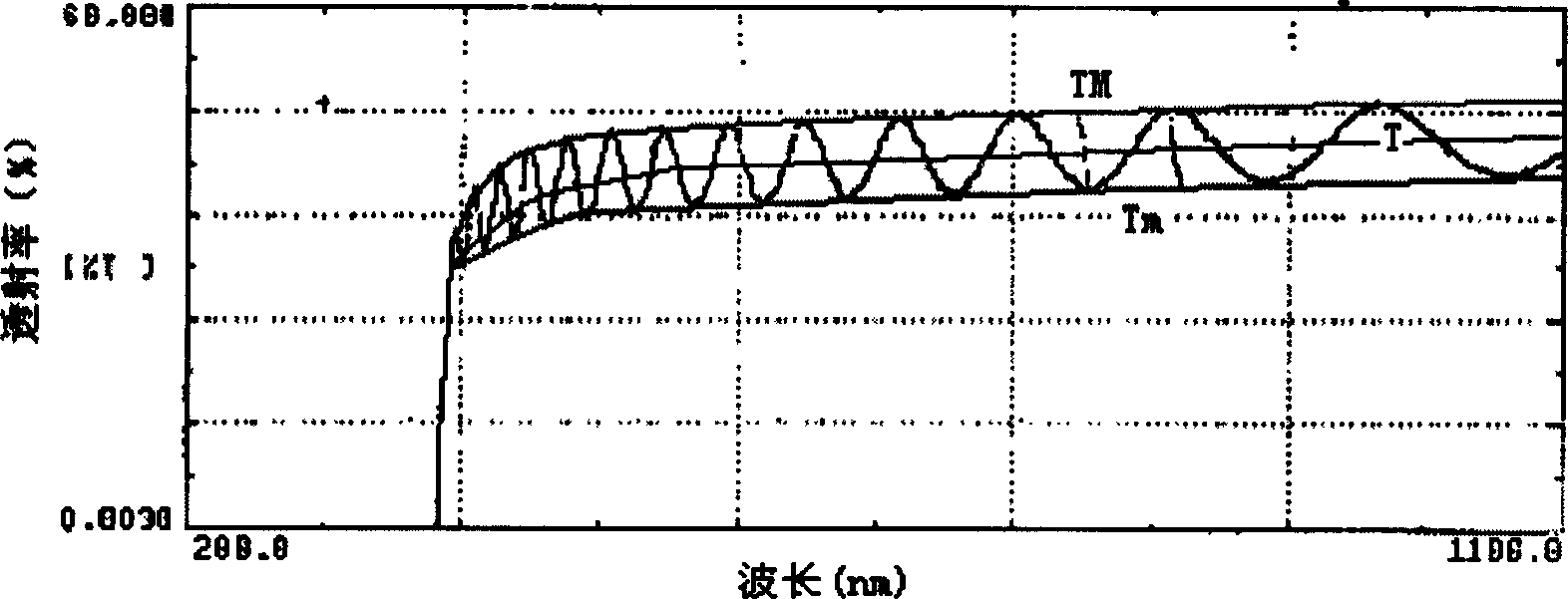
[0099] The specific measurement process of the present invention is illustrated below in conjunction with examples.

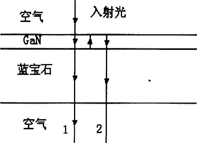
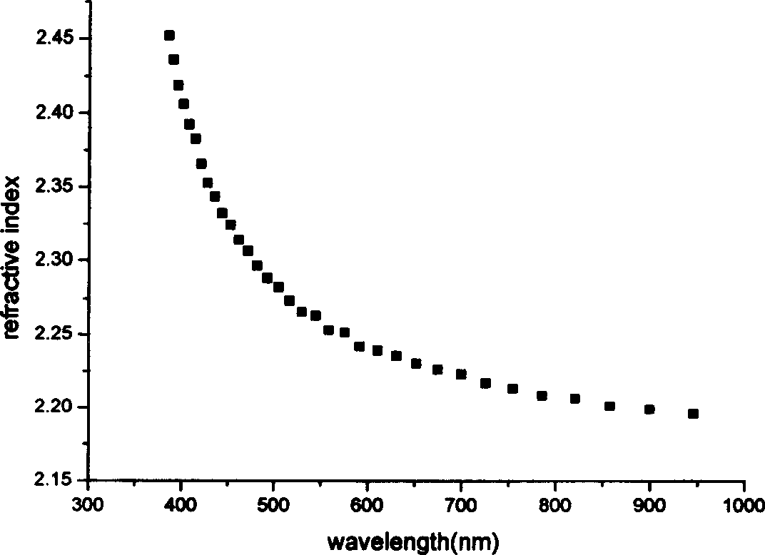
[0100] Metal organic chemical vapor deposition (MOCVD) method is used to epitaxial GaN film material on sapphire substrate, usually sapphire substrate is much thicker than GaN film, the thickness of GaN film is usually between 0.5-5.0μm, and the thickness of sapphire substrate Usually 330μm is tens to hundreds of times of GaN thin film. The refractive index s of the sapphire substrate is known, as shown in Table 1. The absorption coefficient α of sapphire in the measured transmission spectrum range s =0.

[0101] Table 1 Refractive index of sapphire substrate between 355-1064nm

[0102] wavelength

355

442

458

488

515

532

590

633

Refractive index

1.79598

1.78038

1.77843

1.7753

1.77304

1.7717

1.76804

1.7659

[0103] wavelength

...


PUM

PropertyMeasurementUnit
thicknessaaaaaaaaaa
thicknessaaaaaaaaaa

Abstract

The method of measuring the thickness and optical parameters of epitaxial film on single-sided polished substrate is based on the characteristic that the maximum transmissivity of the epitaxial film structure on substrate depends only on the substrate material. The method includes zooming the measured transmissivity extreme values TM and Tm, correcting TM and Tm in considering the effect of the spectral width of the spectrophotometer on the transmissivity to obtain corrected values TM' and Tm', calculating the refractive index n1 of the film in the transparent area and the weak absorption area, and calculating based on the transmissivity extreme value condition the film thickness d1, the average film thickness d, the film refractive index n within the transmissive range and film absorption index alpha. The method is simple and practical.

Description

technical field [0001] The invention belongs to the technical field of measurement and relates to optical measurement of thin films, in particular to a method for measuring the thickness and optical parameters of epitaxial thin films on single-sided polished substrates. When the substrate material is polished on one side and is transparent to the epitaxial material, the thickness and optical parameters of the film are measured by transmission spectrum. Background technique [0002] In the growth of semiconductor materials, epitaxial growth techniques are often used to epitaxially grow thin films on substrates, such as metal organic chemical vapor deposition (MOCVD) growth methods. Many epitaxial thin films grown on substrates, such as polycrystalline Si, GaN, AlGaN, etc., are often used to make optoelectronic devices. In order to predict the performance of the optoelectronic device and design the device better, it is necessary to measure the variation of the refractive inde...

Claims


Application Information

Patent Timeline
Patent Type & Authority Applications(China)
IPC IPC(8): G01B11/06G01N21/41
Inventor 郝跃张春福周小伟
Owner XIDIAN UNIV
Why Eureka
Try Eureka