System and method for mask defect detection

A mask and defect technology, applied in the direction of optical testing flaws/defects, measuring devices, material analysis through optical means, etc., can solve the problems of complex mask layout design and inability to detect mask pattern defects, etc.

Inactive Publication Date: 2006-01-04
TAIWAN SEMICON MFG CO LTD
View PDF0 Cites 0 Cited by
  • Summary
  • Abstract
  • Description
  • Claims
  • Application Information

AI Technical Summary

Problems solved by technology

As the manufacturing process becomes more and more complex, the design of the mask layout is also becoming more and more complicated
[0003] According to the traditional mask defect inspection method, the defect of the exposure pattern can only be detected after the exposure process is executed, and the defect of the mask pattern generated in the preparation stage of the mask data cannot be detected

Method used


Image

  • System and method for mask defect detection
  • System and method for mask defect detection
  • System and method for mask defect detection

Examples


Embodiment Construction

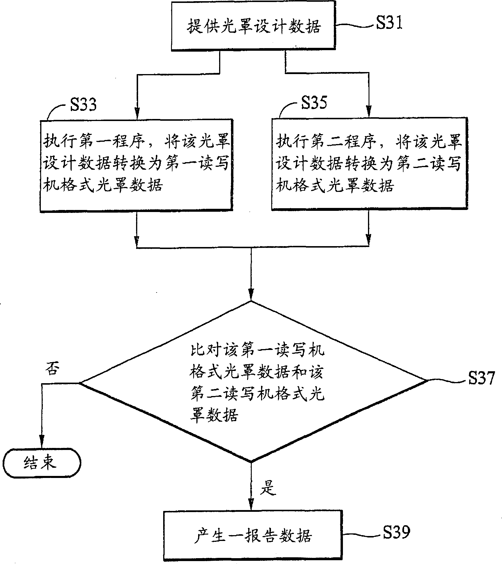
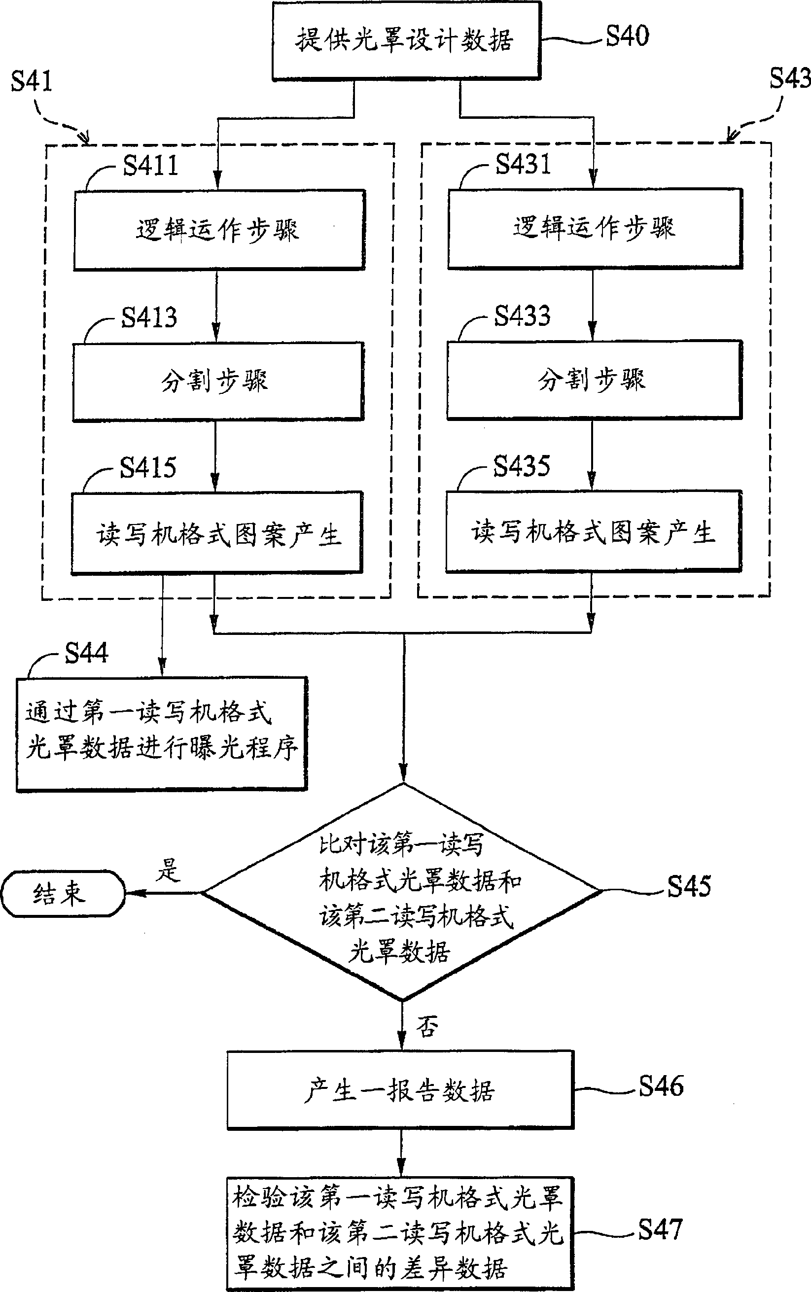
[0023] In order to make the purpose, features and advantages of the present invention more obvious and understandable, the preferred embodiments are specially cited below, together with the attached drawings Figure 1 to Figure 4 , give a detailed explanation. The description of the present invention provides different examples to illustrate the technical features of different implementations of the present invention. Wherein, the configuration of each element in the embodiment is for illustration, not for limiting the present invention. In addition, part of the symbols in the figures in the embodiments are repeated for the purpose of simplifying the description, and do not imply the relationship between different embodiments.

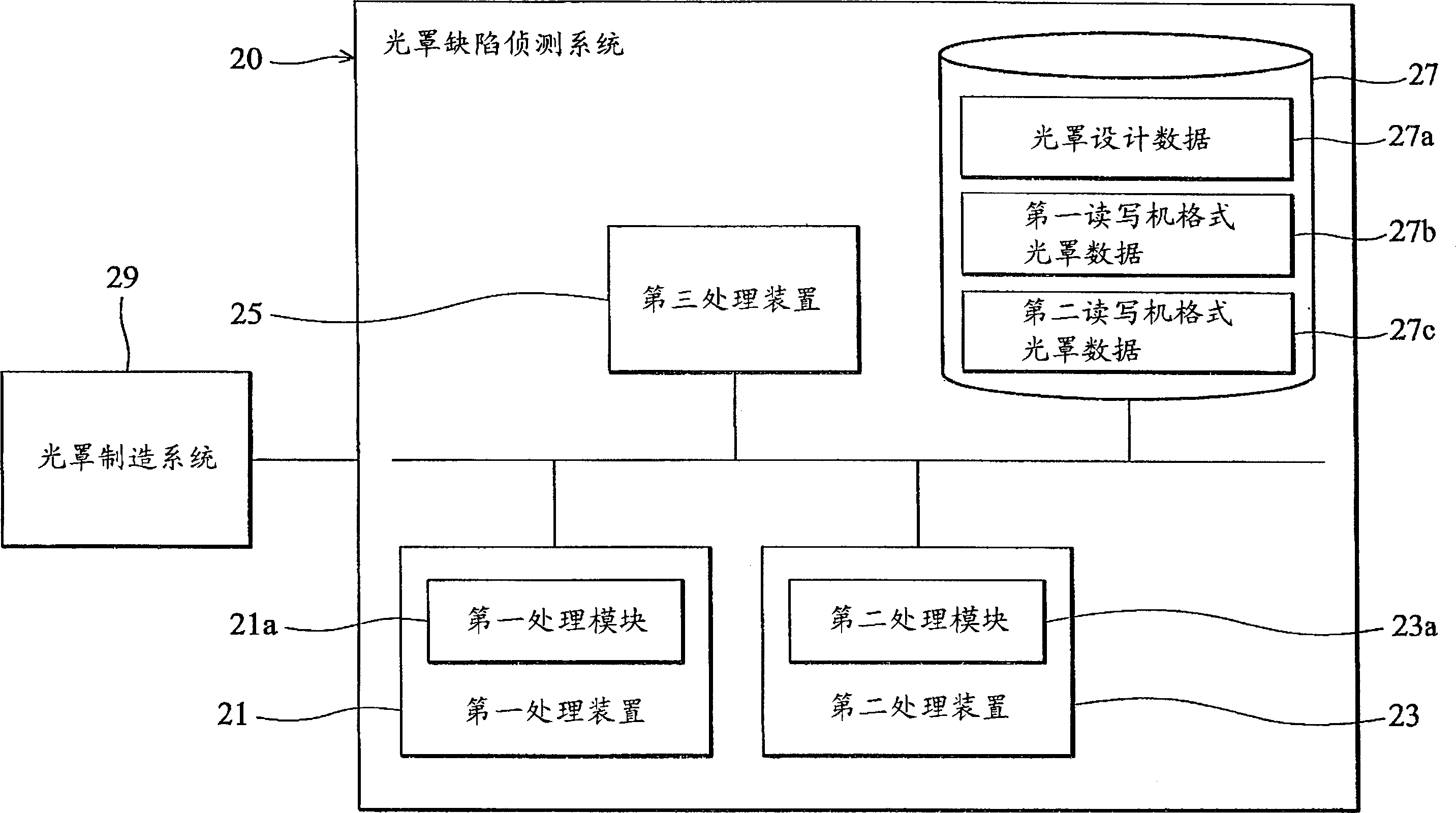
[0024] figure 1 is a schematic diagram showing a mask defect detection system according to an embodiment of the present invention. According to an embodiment of the present invention, the photomask defect detection system 20 is implemented in connec...


PUM


Abstract

The present invention provides a mask defect detection system and a method thereof. The mask defect detection system comprises a first processing device, a second processing device, a third processing device and a storage device. The first processing device is used for transforming a mask design datum into a first read-write device format mask datum, wherein, the first processing device comprises a first processing module. The second processing device is used for transforming the mask design datum into a second read-write device format mask datum, wherein, the second processing device comprises a second processing module which is an object different from the first processing module. The third processing device is used for contrasting the first read-write device format mask datum and the second read-write device format datum, so as to confirm whether difference exists between the first read-write device format mask datum and the second read-write device format datum. The storage device is used for storing the mask datum, the first read-write device format mask datum and the second read-write device format datum.

Description

technical field [0001] The present invention relates to mask defect detection, and more particularly to a system and method for detecting mask defects before an exposure process is performed. Background technique [0002] In recent years, semiconductor integrated circuits (IC) have developed rapidly. With the technological advancement of IC materials and design, the circuit design of IC products has become more and more sophisticated. However, these advances have also made the manufacturing process of ICs increasingly complex. For example, several different circuit devices may have to be included on a single IC. When the size of these circuit devices is reduced to the sub-micron or deep-micron stage, the device density and functional density of ICs are limited by process factors. As the manufacturing process becomes more and more complicated, the design of the mask layout becomes more and more complicated. [0003] According to the traditional mask defect inspection metho...

Claims


Application Information

Patent Timeline
Patent Type & Authority Applications(China)
IPC IPC(8): G01N21/956G01N21/88H01L21/66G06F17/50G06K9/00G06T7/00
CPCG06T7/0004G06T2207/30148
Inventor 周怡儒许志东
Owner TAIWAN SEMICON MFG CO LTD
Why Eureka
Try Eureka