Method for detecting defect of semiconductor elements

A detection method and semiconductor technology, which is applied in the direction of semiconductor/solid-state device testing/measurement, can solve problems such as difficulties, long production time, and inability to detect defects or particles, and achieve time-saving and accurate detection.

Inactive Publication Date: 2005-09-28
POWERCHIP SEMICON CORP
View PDF0 Cites 5 Cited by
  • Summary
  • Abstract
  • Description
  • Claims
  • Application Information

AI Technical Summary

Problems solved by technology

[0004] However, with the increase of semiconductor integration, it will become more and more difficult to detect and analyze the defects of semiconductor components using the above-mentioned method, especially for analyzing the defects caused by the front-end process (such as the defects causing the short circuit between the gate and the plug)
This is because when the above detection method is applied, it needs to be etched layer by layer until the defect is exposed, so it takes a long time to make a test piece that exposes the defect.
Moreover, in the wet etching process of this method, the defects or particles will also be removed by etching, resulting in the defect that the defects or particles cannot be reliably detected.

Method used


Image

  • Method for detecting defect of semiconductor elements
  • Method for detecting defect of semiconductor elements
  • Method for detecting defect of semiconductor elements

Examples


experiment example 1

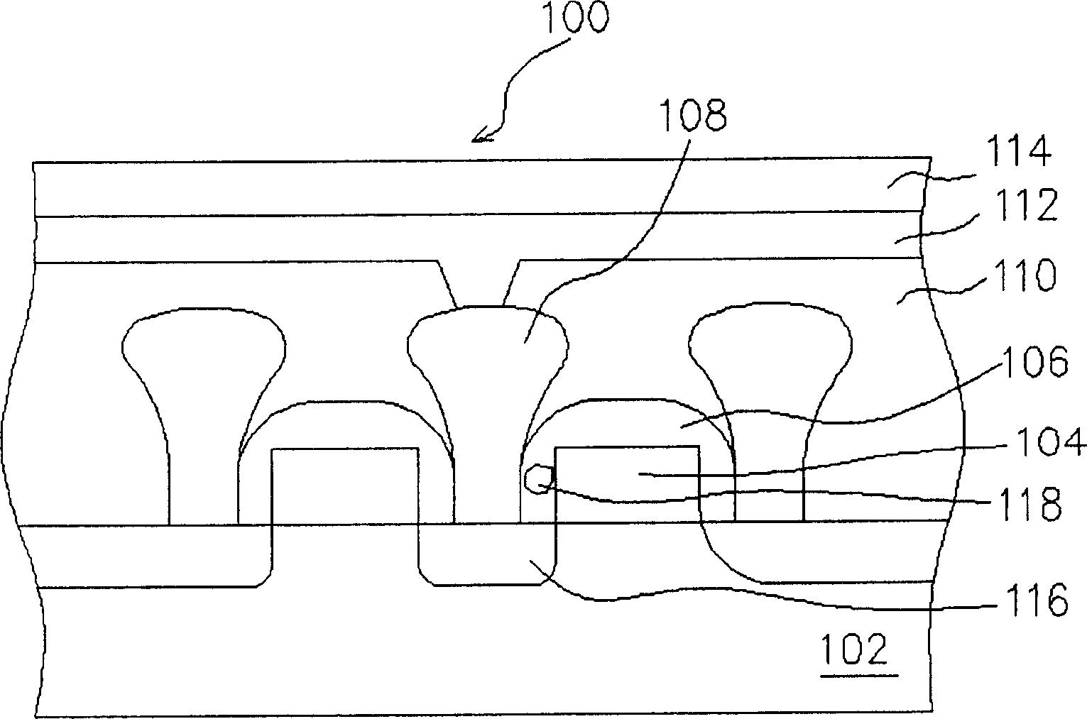
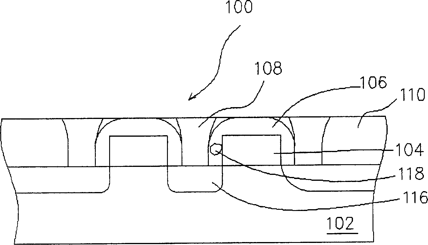
[0037] Provide a semiconductor chip (DRAM) with a line width of 0.15 μm, and perform a grinding step on the semiconductor chip until the plug does not cover the top of the gate. In this grinding step, the grinding time is, for example, about 12 minutes. After the semiconductor chip is cleaned, the insulating layer between the gate and the plug is removed. In this step, for example, a wet etching step is performed first, using hydrofluoric acid (HF) solution as an etchant, and etching is performed for 1 minute. A reactive ion etching process is then performed for 1 minute. A cleaning step is also performed after the insulating layer between the gate and the plug. The semiconductor chip is then inspected using a scanning electron microscope. The result is as Figure 2A and Figure 2B As shown (the part in the figure is the storage unit area of ​​the DRAM).

experiment example 2

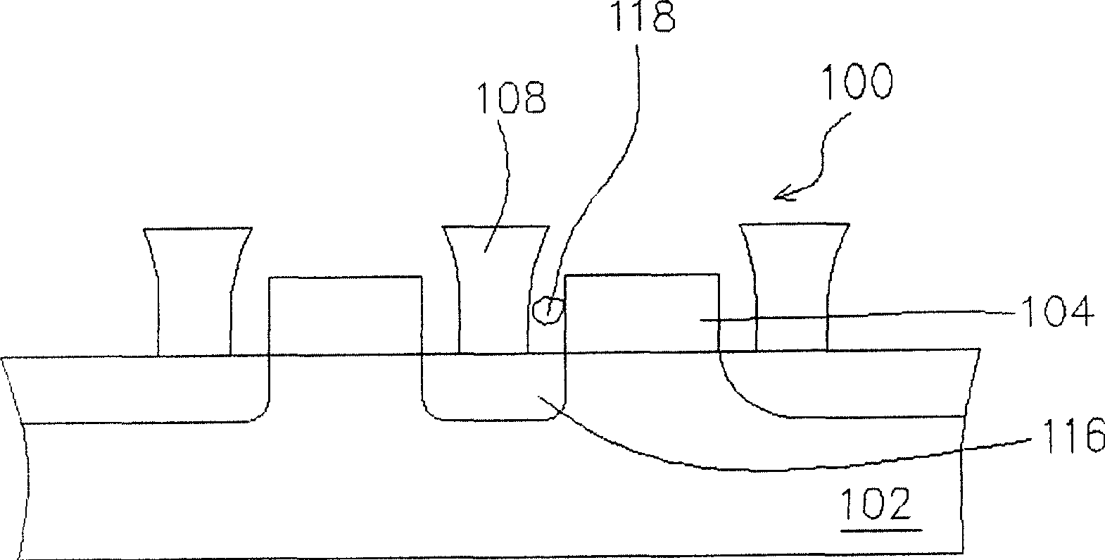
[0039] Provide a semiconductor chip (DRAM) with a line width of 0.13 μm, and then perform the same process steps as in Experimental Example 1 on this semiconductor chip, and then use a scanning electron microscope to detect this semiconductor chip. The result is as Figure 3A and Figure 3B As shown (the part in the figure is the storage unit area of ​​the DRAM).


PUM


Abstract

A detection method of semiconductor element defect includes providing a semiconductor element consisting of substrate, grid, plug, insulation layer and wire; having plug connected in electricity to source electrode / drain electrode area in substrate at two sides of grid and having it partially covered above grid as well as having defect done between plug and grid; grinding semiconductor element to position above grid uncovered by play; washing semiconductor element; moving off insulation layer between plug and grid to detect the defect there.

Description

technical field [0001] The invention relates to a detection method of a semiconductor element, and in particular to a detection method of a semiconductor element defect. Background technique [0002] The so-called integrated circuit is an electronic product that reduces and manufactures various components and circuits required for a specific circuit in an area of ​​only 2 cm or less. Because integrated circuits are mostly composed of tens of thousands of solid-state electronic components whose size can only be viewed with a microscope, they can also be called microelectronic components. If there is a defect in the above-mentioned microelectronic element, it will cause the failure of the electronic device formed by the microelectronic element. Moreover, when the semiconductor design specifications shrink, it is more difficult to improve and maintain the yield rate of the semiconductor process, and defects are the most important key to affect the process yield. Therefore, th...

Claims


Application Information

Patent Timeline
Patent Type & Authority Applications(China)
IPC IPC(8): H01L21/66
Inventor 张宏嘉张圣如
Owner POWERCHIP SEMICON CORP
Why Eureka
Try Eureka