One-time programmable memory device
A storage device and programming device technology, which is applied in the field of one-time programmable storage devices, can solve problems such as transistor damage, and achieve the effect of low cost and low selection
- Summary
- Abstract
- Description
- Claims
- Application Information
AI Technical Summary
Problems solved by technology
Method used
Image


Examples
Embodiment Construction
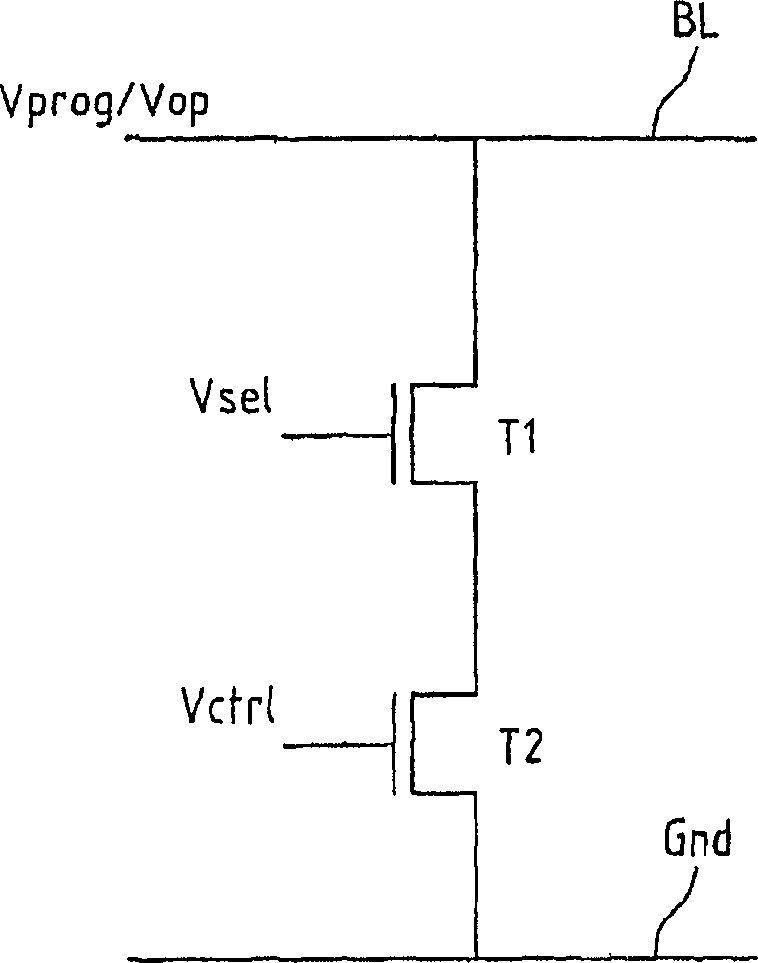
[0023] figure 1 An OTP memory cell forming part of a CMOS memory device according to the invention is shown. The memory cell includes a selection transistor T1 and a storage transistor T2. Both transistors T1 and T2 are NMOS transistors. The drain of the selection transistor T1 is connected to the bit line BL, and the gate of the selection transistor T1 is connected to a voltage source (not shown) supplying a voltage Vsel. The source of the selection transistor T1 is connected to the drain of the storage transistor T2, and the source of the storage transistor T2 is connected to the ground Gnd. The gate of the storage transistor T2 is connected to a voltage source (not shown) that provides a voltage Vctrl.
[0024] In the unprogrammed state of the memory cell, the drain junction of the storage transistor T2 is undamaged, while in the programmed state of the memory cell, the drain junction of the storage transistor T2 is thermally damaged.
[0025] To program the memory cell...
PUM
 Abstract
Description
Claims
Application Information