Unlock instant, AI-driven research and patent intelligence for your innovation.

Array substrate, manufacturing method thereof, and display device

A technology of an array substrate and a manufacturing method, applied in the display field, can solve the problems of lack of buffer layer, product quality risk, contamination of film layer structure, etc., and achieve the effect of reducing the area and avoiding unstable product performance

Active Publication Date: 2020-06-12
HEFEI XINSHENG OPTOELECTRONICS TECH CO LTD +1
View PDF11 Cites 0 Cited by
  • Summary
  • Abstract
  • Description
  • Claims
  • Application Information

AI Technical Summary

Problems solved by technology

However, the organic film may decompose during use and pollute its adjacent film layer structure. In order to solve this problem, a buffer layer is generally placed under the organic film, but the buffer layer is not formed due to abnormal equipment or process errors. , it will cause product quality risk, therefore, it is necessary to detect the defect of missing buffer layer in time

Method used


Image

  • Array substrate, manufacturing method thereof, and display device
  • Array substrate, manufacturing method thereof, and display device
  • Array substrate, manufacturing method thereof, and display device

Examples


Embodiment Construction

[0032] The application will be further described in detail below in conjunction with the accompanying drawings and embodiments. It should be understood that the specific embodiments described here are only used to explain related inventions, rather than to limit the invention. It should also be noted that, for ease of description, only parts related to the invention are shown in the drawings.

[0033] It should be noted that, in the case of no conflict, the embodiments in the present application and the features in the embodiments can be combined with each other. The present application will be described in detail below with reference to the accompanying drawings and embodiments.

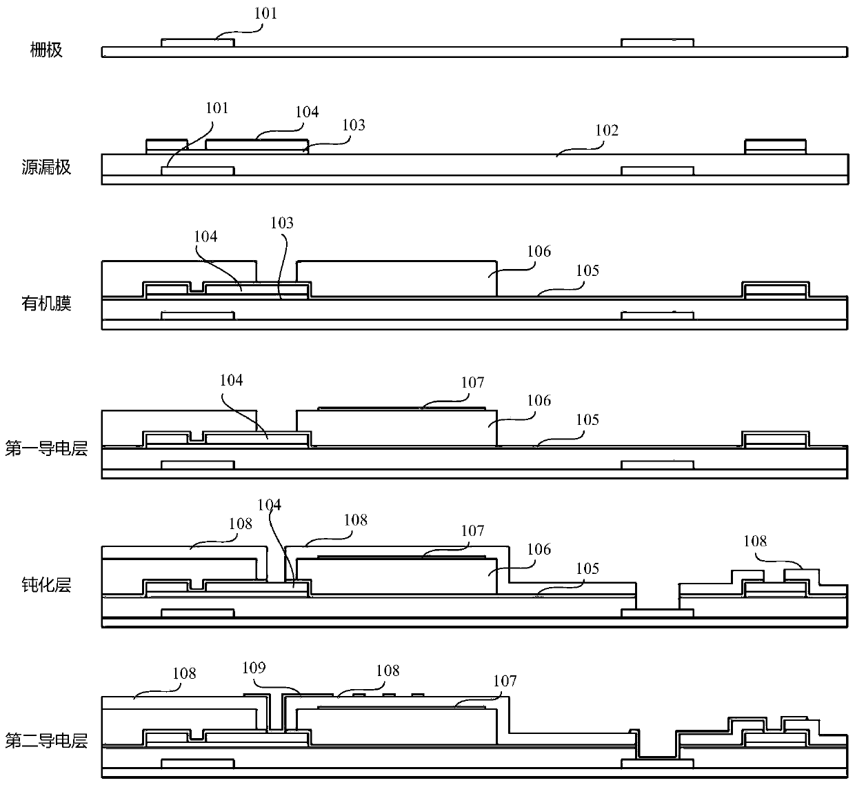
[0034] figure 1 It is a schematic diagram of a manufacturing process flow of an array substrate including an organic film in a related art. Such as figure 1 As shown, the manufacturing process flow includes 6 masking processes, including the following process flow in sequence: gate (Gate), sourc...


PUM


Abstract

The invention provides an array substrate, a manufacturing method thereof, and a display device. The manufacturing method includes: arranging a plurality of detection pixel units on the substrate. The manufacturing method of the detection pixel unit includes: forming at least two data lines, forming a buffer layer on the data lines; forming an organic film provided with a via hole on the buffer layer; The orthographic projections on the substrate are partially overlapped; and a first conductive layer is formed on the organic film. Wherein, when the formation of the buffer layer fails, the first conductive layer short-circuits the adjacent data line through the via hole. In the array substrate and its manufacturing method and display device provided by the present invention, via holes covering adjacent data lines are provided on the organic film, so that the first conductive layer can short-circuit the adjacent data lines through the via holes when the formation of the buffer layer fails. Data lines, so as to detect the short-circuit signal of adjacent data lines in the array detection, and detect the problem of missing buffer layer, so as to avoid hidden dangers of product quality risks.

Description

technical field [0001] The present application relates to the field of display technology, in particular to an array substrate, a manufacturing method thereof, and a display device. Background technique [0002] The use of organic film technology can effectively reduce the coupling capacitance between the data line and the common electrode, increase the aperture ratio of the product, thereby reducing the power consumption of the thin film transistor liquid crystal display, and has been widely used in recent years. However, the organic film may decompose during use and pollute its adjacent film layer structure. In order to solve this problem, a buffer layer is generally placed under the organic film, but the buffer layer is not formed due to abnormal equipment or process errors. , it will cause the quality risk of the product, therefore, it is necessary to detect the defects of the missing buffer layer in time. Contents of the invention [0003] In view of the above-mentio...

Claims


Application Information

Patent Timeline
Patent Type & Authority Patents(China)
IPC IPC(8): G02F1/1333G02F1/1362
CPCG02F1/1333G02F1/1362G02F1/136254H10K59/87H01L27/124H01L27/1262G09G3/20H10K59/124H10K50/84
Inventor 操彬彬张辉艾力
Owner HEFEI XINSHENG OPTOELECTRONICS TECH CO LTD
Features
  • R&D
  • Intellectual Property
  • Life Sciences
  • Materials
  • Tech Scout
  • Unparalleled Data Quality
  • Higher Quality Content
  • 60% Fewer Hallucinations
Learn More