Exposure apparatus and method for producing device

An exposure device and exposed technology, used in semiconductor/solid-state device manufacturing, photolithographic process exposure devices, microlithography exposure equipment, etc., can solve the problems of rust, inability to maintain cleanliness, and failure to obtain pattern transfer accuracy. , to achieve the effect of inhibiting diffusion

Inactive Publication Date: 2006-01-18
NIKON CORP
View PDF16 Cites 4 Cited by
  • Summary
  • Abstract
  • Description
  • Claims
  • Application Information

AI Technical Summary

Problems solved by technology

If the transfer is carried out with the remaining liquid attached to the substrate, the liquid will fall from the substrate during the transfer, and the devices or components around the transfer path will be rusted by the dropped liquid, and the arrangement cannot be maintained. Defects such as the cleanliness of the device environment will occur
Or, there is a case where the environment around the exposure device changes (humidity change) due to the dropped liquid
If the humidity changes, for example, there will be fluctuations in the air on the optical path of the optical interferometer used in the stage position measurement, and the stage position measurement will not be performed with good accuracy, and the desired pattern transfer accuracy will not be obtained. questions like
In addition, if, for example, a development process is performed with the liquid attached to the substrate after the exposure process, there is a possibility that a device with desired performance cannot be manufactured.

Method used


Image

  • Exposure apparatus and method for producing device
  • Exposure apparatus and method for producing device
  • Exposure apparatus and method for producing device

Examples


no. 1 Embodiment approach

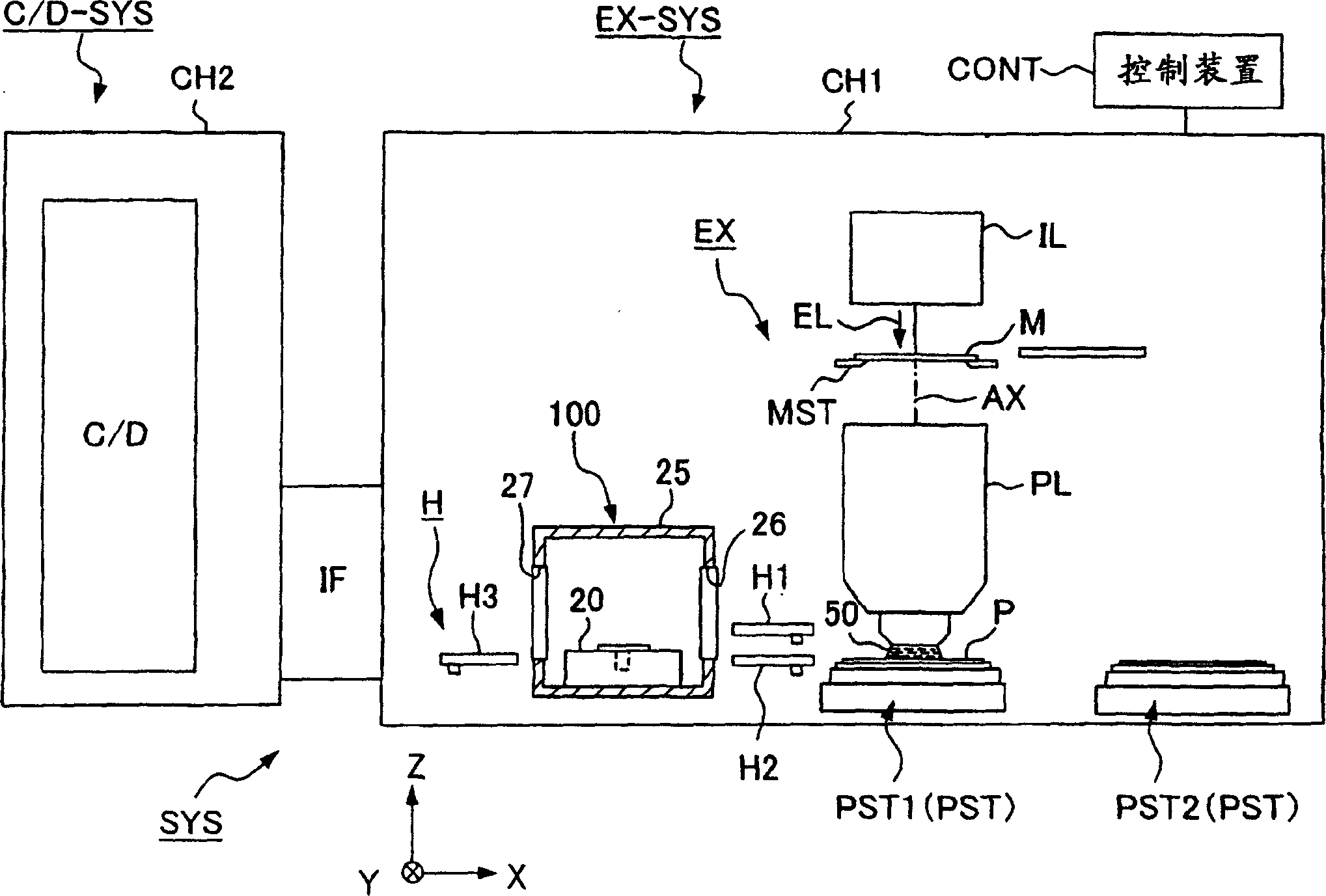
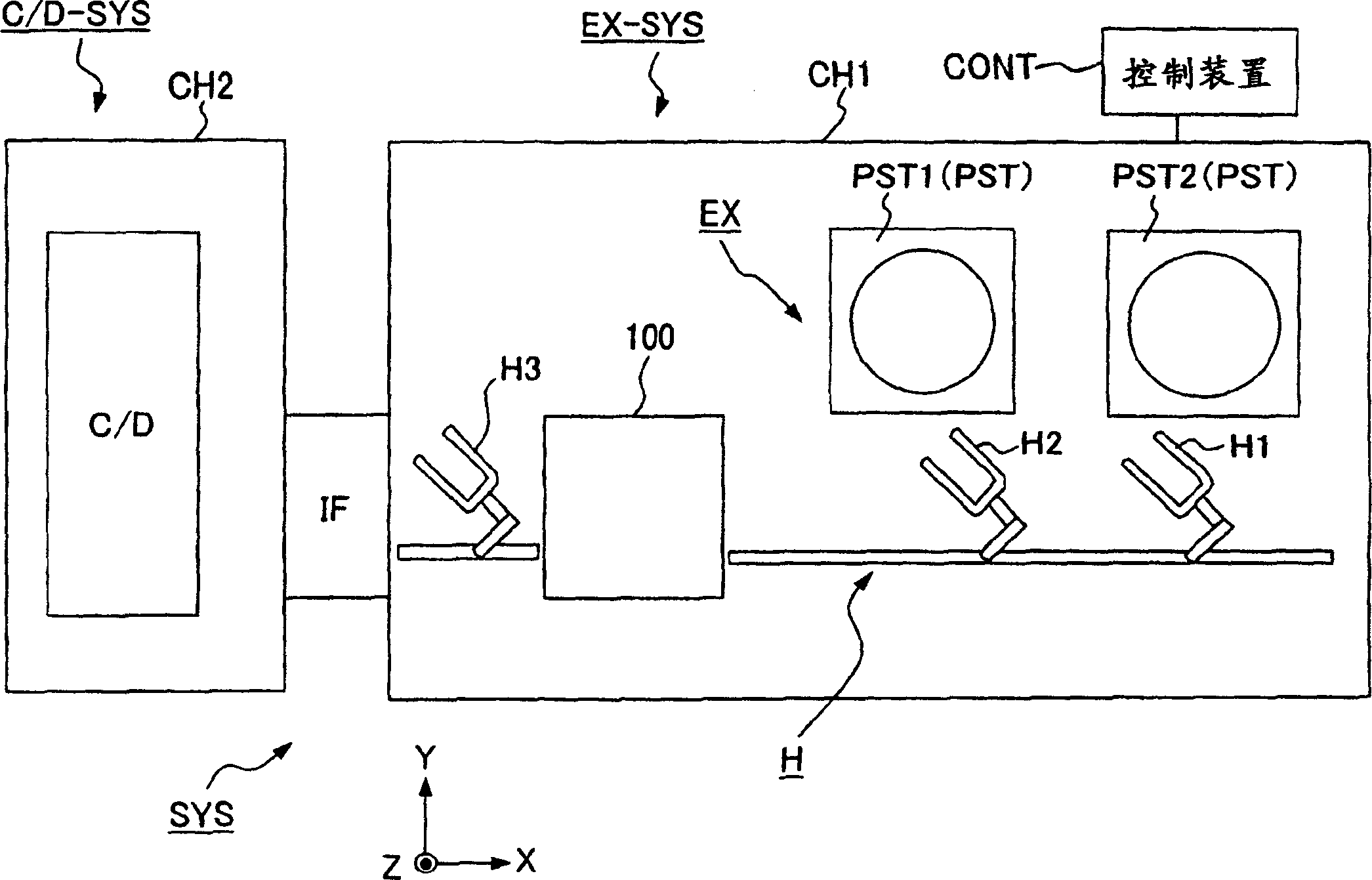
[0047] Below, while referring to the attached Figure 1 Next, the exposure apparatus and device manufacturing method of the present invention will be described. figure 1 It is a figure which shows one embodiment of the device manufacturing system which has the exposure apparatus of this invention, and the schematic structural figure seen from the side, figure 2 is viewed from above figure 1 diagram.

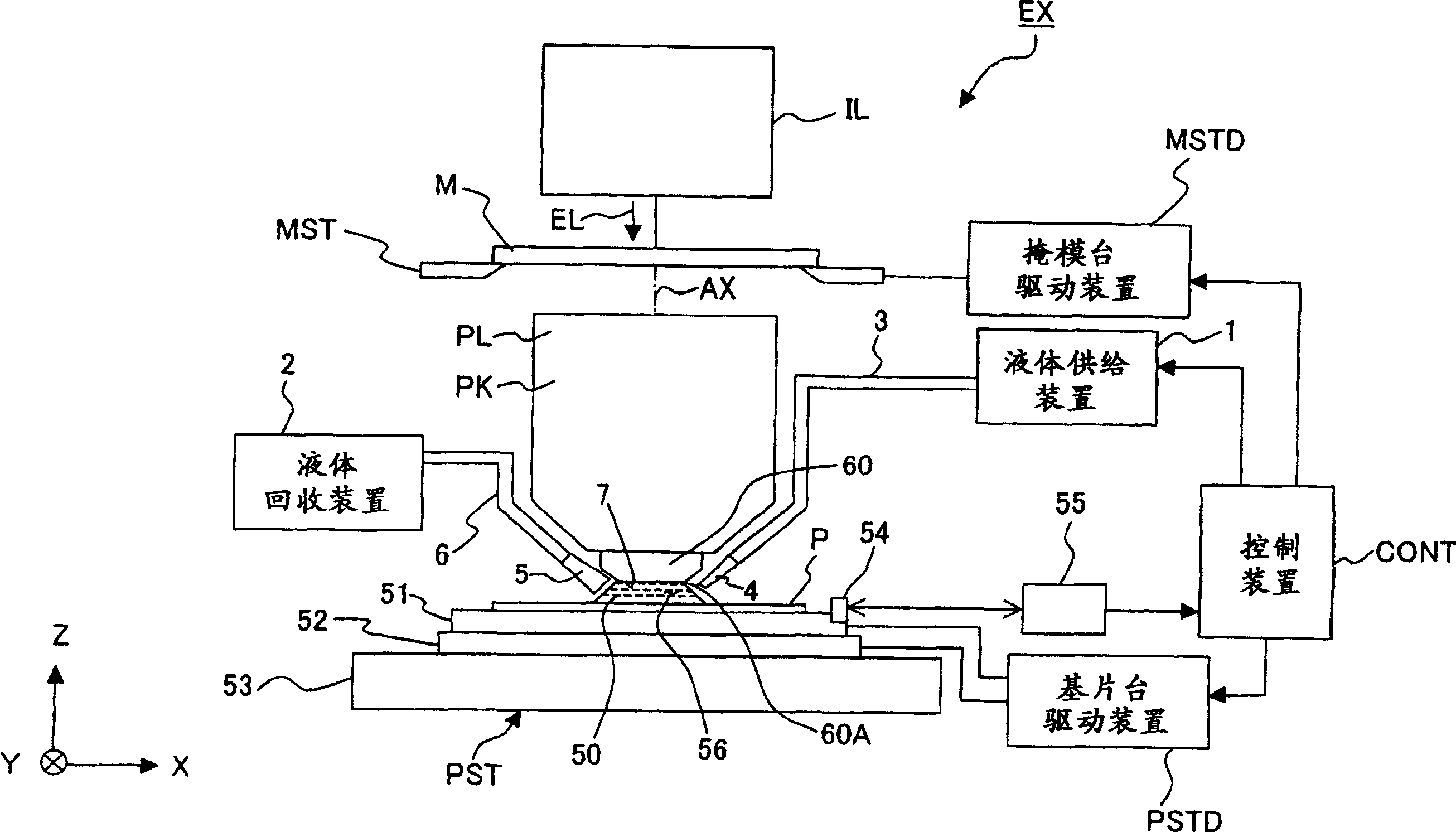
[0048] exist figure 1 , figure 2 Among them, the device manufacturing system SYS has an exposure device EX-SYS and a coater / developer device C / D-SYS. The exposure device EX-SYS has: an interface part IF forming a connection part with the applicator-developer device C / D-SYS, and the space between the projection optical system PL and the substrate P is filled with liquid 50, and the projection optical system PL PL and the liquid 50 project a pattern image onto the substrate P and expose the substrate P to the exposure apparatus body EX, and a transfer system H for transfe...

no. 2 Embodiment approach

[0085] Next, the liquid removal device 100 used in the exposure device according to the second embodiment of the present invention will be described with reference to FIG. 6 . Here, in the following description, descriptions other than the liquid removal device 100 are simplified or omitted because they are the same or equivalent to those of the first embodiment.

[0086] In FIG. 6, the liquid removal device 100 is provided with a cover portion (cover) constituting a part of a cover mechanism covering the periphery of the substrate P in order to prevent the liquid 50 from splashing when removing the liquid 50 attached to the substrate P. )30. The liquid removal device 100 in this embodiment does not have the chamber 25 . The cover portion 30 is formed in a substantially annular shape in plan view, and has a pocket portion 30A inside the annular ring. The liquid suction device 29 is connected to the groove portion 30A of the cover portion 30 . Moreover, the cover part 30 can...

no. 3 Embodiment approach

[0089] Next, while referring to Figure 7 The liquid removal device 100 used in the exposure device of the third embodiment will be described. The characteristic part of this embodiment is that the rotation mechanism 22 and the cover part 30 constituting the liquid removal apparatus 100 are provided on the substrate stage PST of the exposure apparatus body EX that performs exposure processing. Since the structure of the exposure apparatus main body EX is the same as that of the first embodiment, description thereof will be omitted.

[0090] exist Figure 7 In (a), the substrate stage PST has the holder part 21 and the second holder part 24 which hold the substrate P, and the recessed part 31 which can accommodate the cover part 30. As shown in FIG. Then, if Figure 7 As shown in (a), the pattern image is transferred to the substrate P held on the holder unit 21 and the second holder unit 24 through the projection optical system PL and the liquid 50 . Once the exposure proc...


PUM

PropertyMeasurementUnit
refractive indexaaaaaaaaaa

Abstract

An exposure apparatus which performs an exposure while filling a space between a projection optical system and a substrate with a liquid, and in which deterioration of a device caused by adherent liquid on the substrate is suppressed is provided. A device manufacturing system (SYS) includes a main body of an exposure apparatus (EX) which fills a space between a projection optical system (PL) and a substrate (P)with a liquid (50) and projects an image of a pattern onto the substrate (P) via the projection optical system (PL) and the liquid (50); an interface section (IF) which is arranged between the exposure apparatus main body (EX) and a coater/developer main body (C/D) which processes the substrate (P) after exposure; and a liquid-removing unit (100) which removes the liquid (50) adhering to the substrate (P) before the exposed substrate (P) is transferred into the coater/developer main body (C/D) through the interface section (IF).

Description

technical field [0001] The present invention relates to an exposure device for exposing a substrate by filling at least a portion between a projection optical system and a substrate with a liquid, using a pattern image projected by the projection optical system, a liquid removal device used in the exposure device, and an exposure device using the exposure device. Device fabrication methods. Background technique [0002] A semiconductor device or a liquid crystal display device is manufactured by a method called photolithography in which a pattern formed on a mask is transferred to a photosensitive substrate. The exposure apparatus used in this photolithography process has a mask stage that supports the mask and a substrate stage that supports the substrate. While moving the mask stage and the substrate stage one by one, the pattern of the mask is projected through the projection optical system. Transfer to substrate. In recent years, in order to cope with higher integratio...

Claims


Application Information

Patent Timeline
Patent Type & Authority Applications(China)
IPC IPC(8): H01L21/027G03F7/20
Inventor 马込伸贵高岩宏明荒井大
Owner NIKON CORP
Why Eureka
Try Eureka