Photodetector

a technology of photodetector and resonator, which is applied in the direction of optical radiation measurement, radiation control devices, instruments, etc., can solve the problems of increasing production costs, and achieve the effect of curb deterioration in a common-mode rejection ratio

Pending Publication Date: 2022-03-10
NIPPON TELEGRAPH & TELEPHONE CORP
View PDF0 Cites 0 Cited by
  • Summary
  • Abstract
  • Description
  • Claims
  • Application Information

AI Technical Summary

Benefits of technology

[0021]The present invention can make plural Ge PDs uniform in sensitivity by heating the Ge PDs with heaters based on photocurrent measurements taken by the current monitor, and thereby curb deterioration in a common-mode rejection ratio.

Problems solved by technology

If one attempts to incorporate a Ge PD whose sensitivity varies with the temperature and wavelength into an optical communications system, a circuit for use to compensate for the sensitivity variation becomes necessary, increasing production cost.

Method used


Image

  • Photodetector
  • Photodetector
  • Photodetector

Examples


embodiment 1

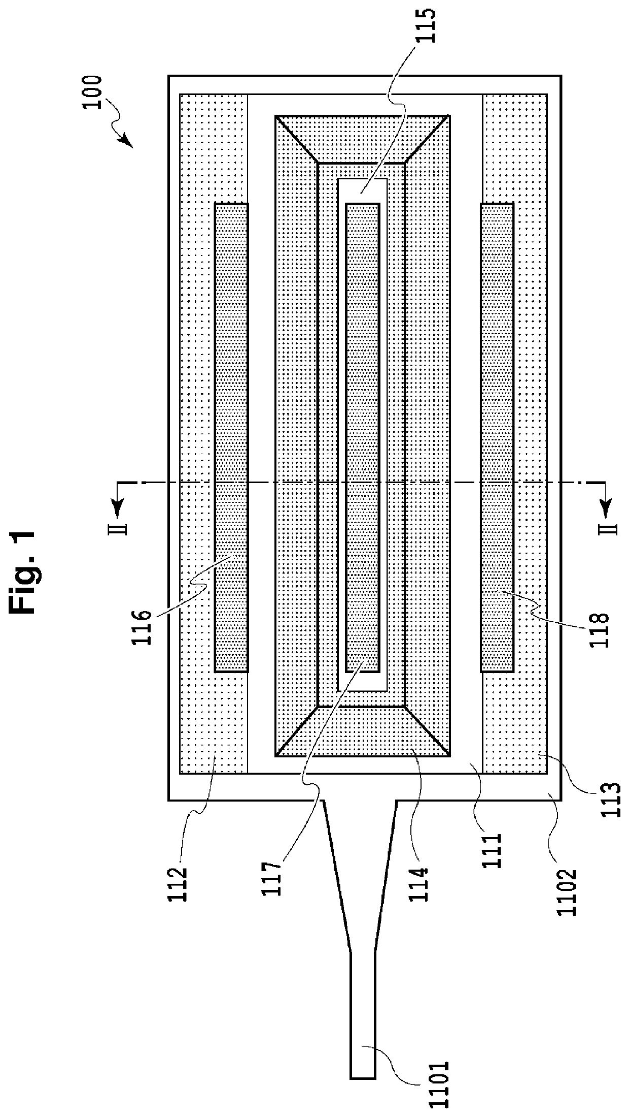
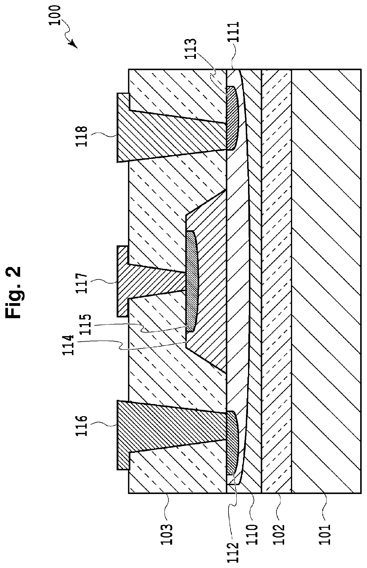
[0037]FIGS. 9 and 10 are a top view and a sectional view, respectively, showing a configuration of a first embodiment of the photodetector according to the present invention. In this example, ammeters connected to the cathodes of the Ge PDs 1001 and 1002 serve as monitors while the heaters 200 and 201 containing a metal or metal compound are placed as resistors. As shown in FIG. 9, a photodetector according to the present invention includes two or more photodiodes (Ge PDs) 1001 and 1002 placed to receive an input differential signal; ammeters 204 and 205 serving as current monitors adapted to measure photocurrents of the two or more photodiodes; heaters 200 and 201, which are resistors adapted to heat the photodiodes; and voltage sources 202 and 203 connected to the respective resistors to control the resistors and capable of controlling voltage values independently of each other. Here, the voltage source 202 is connected with the ammeter 204 serving as a current monitor, the volta...

embodiment 2

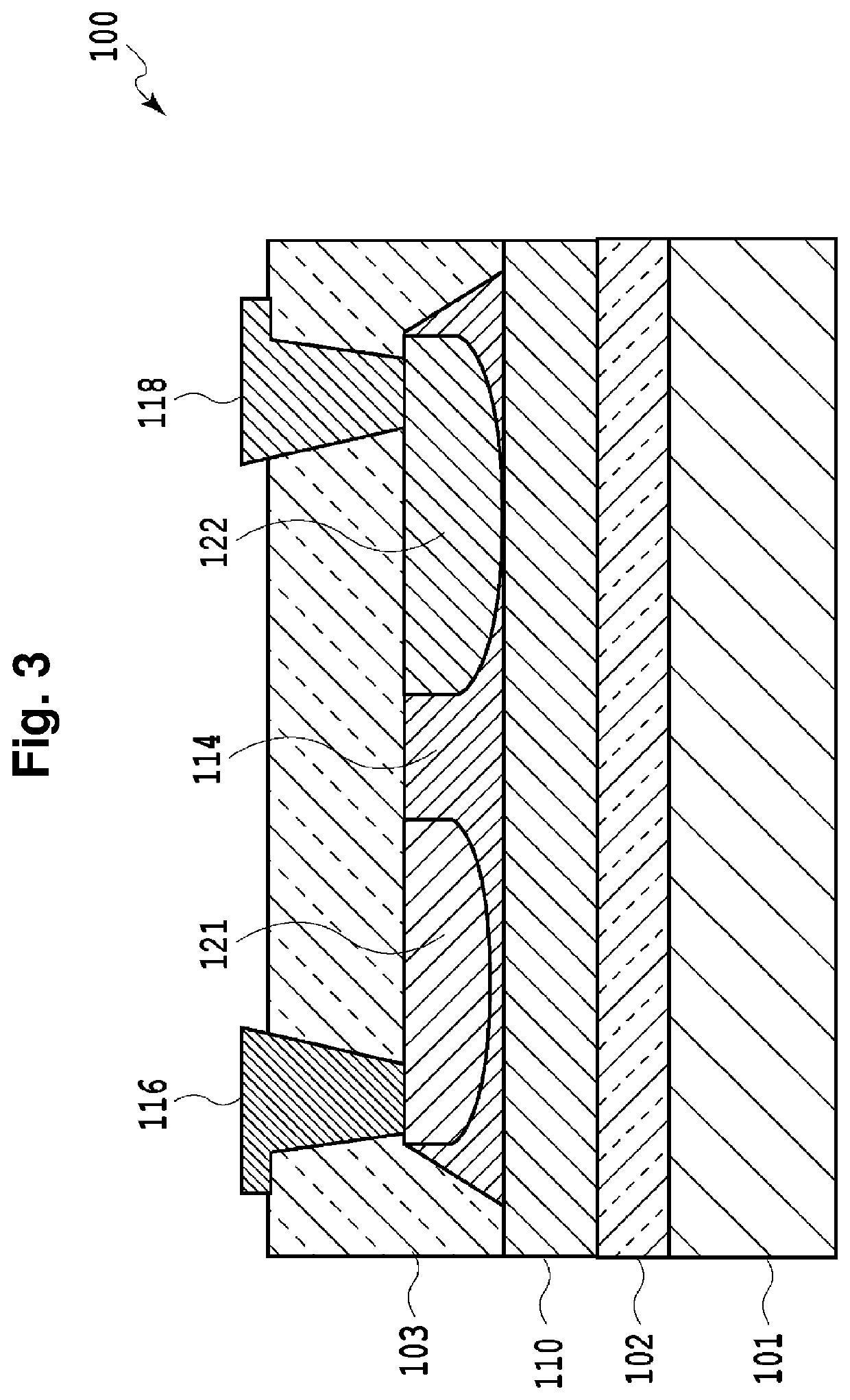
[0038]FIG. 11 is a diagram showing a configuration of a second embodiment of the photodetector according to the present invention. In this example, ammeters connected to the cathodes of the Ge PDs 1001 and 1002 serve as monitors while heaters 210 and 211 created by implantation (ion implantation) in the core layers 110 of the Ge PDs 1001 and 1002 are placed as resistors. The Ge PDs 1001 and 1002 are placed as a PD pair to receive a differential signal. The ammeters 204 and 205 are attached to the cathodes of the respective Ge PDs, and voltage sources 206 and 207 are connected to the ammeters 204 and 205, respectively. The ammeters 204 and 205 are connected, respectively, with the voltage sources 202 and 203 for the respective heaters 200 and 201. The voltage sources 202 and 203 adjust the voltages applied to the heaters, such that the currents indicated by the ammeters 204 and 205 will be equal to each other.

embodiment 3

[0039]FIG. 12 is a diagram showing a configuration of a third embodiment of the photodetector according to the present invention. In this example, a transimpedance amplifier 220 connected to the anodes of the Ge PDs 1001 and 1002 serve as a monitor while the heaters 200 and 201 containing a metal or metal compound are placed as resistors. The Ge PDs 1001 and 1002 are placed as a PD pair to receive a differential signal. The transimpedance amplifier 220 amplifies Ge PD signals and produces voltage output while monitoring currents from the Ge PDs. The transimpedance amplifier 220 feeds values of the currents back to the voltage sources 202 and 203, which then control the heaters such that currents entering the transimpedance amplifier 220 from the Ge PDs will be equal to each other. Whereas the heaters made of a metal or metal compound are used as resistors in FIG. 12, heaters created by implantation (ion implantation) in the core layers 110 of the Ge PDs 1001 and 1002 may be used as...


PUM

PropertyMeasurementUnit
wavelength rangesaaaaaaaaaa
photocurrentsaaaaaaaaaa

Abstract

A problem to be solved is to make plural Ge PDs uniform in sensitivity by heating the Ge PDs with heaters based on photocurrent measurements taken by a current monitor, and thereby curb deterioration in a common-mode rejection ratio. A photodetector according to the present invention is a germanium photodetector (Ge PD) that uses germanium or a germanium compound in a light absorption layer, the photodetector including two or more Ge PDs placed to receive an input differential signal; a current monitor adapted to measure photocurrents of the two or more Ge PDs; resistors adapted to heat the respective Ge PDs; voltage sources connected to the respective resistors and capable of controlling voltage values independently of each other, wherein the voltage sources are connected with the current monitor, and the voltage sources manipulate voltages applied to the heaters such that current values output by the two or more Ge PDs will match each other.

Description

TECHNICAL FIELD[0001]The present invention relates to a photodetector used in an optical communications system and an optical information processing system, and more particularly, to a structure used to provide a photodetector having a small common-mode rejection ratio in receiving a differential signal.BACKGROUND ART[0002]With the recent spread of optical communications, there has been demand for cost reduction of optical communications devices.[0003]One of solutions to this is a method that forms an optical circuit of an optical communications device on a large-diameter wafer such as a silicon wafer using a microoptical circuit technique such as silicon photonics. This dramatically reduces material costs per chip, making it possible to reduce the costs of optical communications devices. [0004]A typical photodetector formed on a silicon (Si) substrate that uses such a technique is a germanium photodetector (Ge PD) that lends itself to monolithic integration. FIG. 1 is a diagram sch...

Claims


Application Information

Patent Timeline
Patent Type & Authority Applications(United States)
IPC IPC(8): H01L27/146H01L31/028G01J1/42H01L31/0232
CPCH01L27/14643H01L31/0232G01J1/42H01L31/028H01L27/1446G01J1/1626H01L31/1808H01L31/1864H01L31/035281H01L31/105
Inventor TAKEDA, KOTARO
Owner NIPPON TELEGRAPH & TELEPHONE CORP
Why Eureka
Try Eureka