SiGe strain relaxed buffer for high mobility devices and a method of fabricating it

A buffer layer and device technology, applied in semiconductor/solid-state device manufacturing, semiconductor devices, electrical components, etc., can solve problems such as material consumption, low-line dislocation, and non-active device areas

Active Publication Date: 2006-01-18
INTERUNIVERSITAIR MICRO ELECTRONICS CENT (IMEC VZW) +1
View PDF1 Cites 5 Cited by
  • Summary
  • Abstract
  • Description
  • Claims
  • Application Information

AI Technical Summary

Problems solved by technology

[0008] Although relatively high mobility and low threading dislocation density can be achieved, thick graded buffer layers still exhibit some more economical and technical disadvantages: growth time, material consumption, for microelectronics with Si Excessive step height for device integration
SRB may not be part of active device area

Method used


Image

  • SiGe strain relaxed buffer for high mobility devices and a method of fabricating it
  • SiGe strain relaxed buffer for high mobility devices and a method of fabricating it
  • SiGe strain relaxed buffer for high mobility devices and a method of fabricating it

Examples


Embodiment Construction

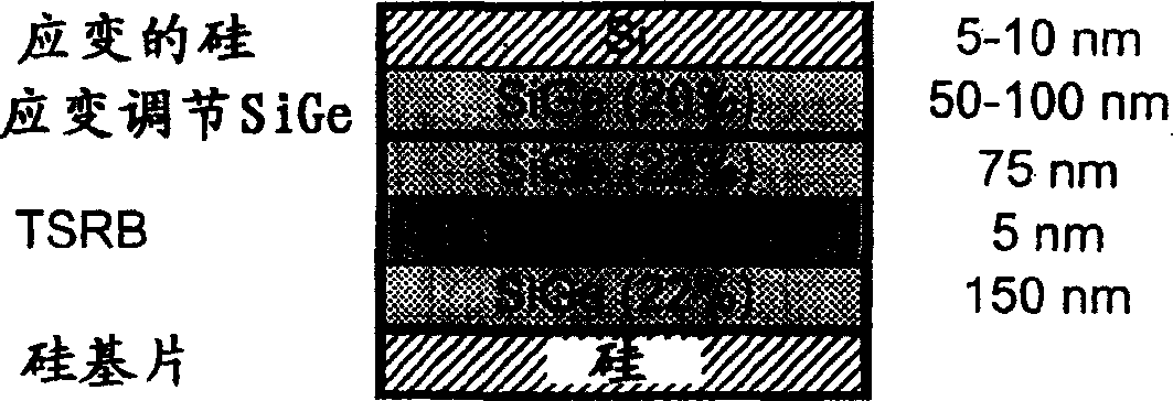
[0055] The present invention relates to a Thin Strain Relaxation Buffer (TSRB) for the integration of high mobility devices (eg SiGe / strained Si systems) on top of a semiconductor substrate such as silicon. In the following description, thin strain buffer layers and methods for obtaining them are explained.

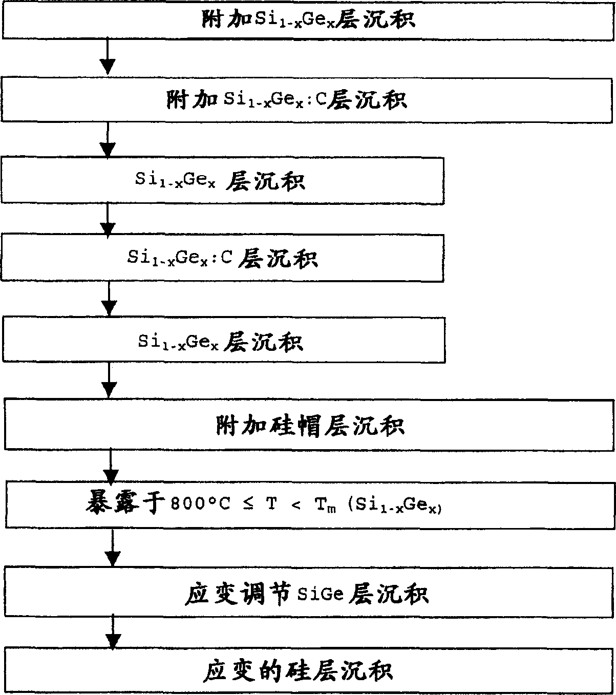
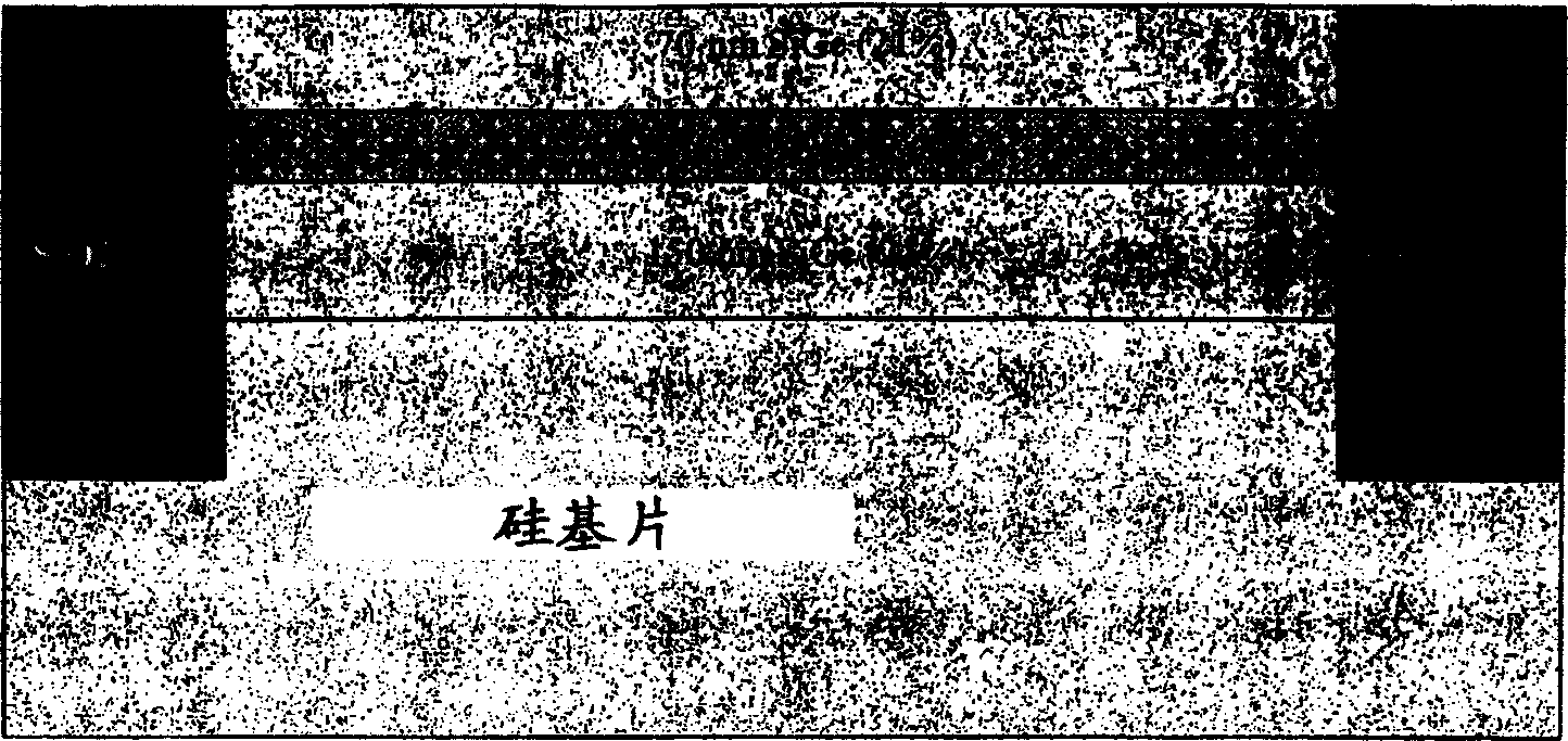
[0056] in Si 0.78 Ge 0.22 / Si 0.78 Ge 0.22 :C y / Si 0.78 Ge 0.22 Epitaxial growth of TSRB on the basis of a multilayer system with a y (C concentration) of at least 0.3%, preferably between 0.5% and 1%, yielded 91% after rapid thermal annealing (30" at 1000°C) of Relaxed, with a very smooth surface (RMS-1 nm). No dislocations reaching the surface of the epitaxial layer were observed. To create heterocenters for dislocation nucleation, carbon was introduced during the growth of SiGe with the in situ method.

[0057] figure 1 shows the complete structure of a 230 nm TSRB on a silicon substrate with a SiGe / Si heterosystem deposited on top according to the present inv...


PUM


Abstract

The invention relates to a semiconductor device comprising a semiconductor substrate and having on its top at least a Thin Strain Relaxed Buffer, consisting essentially of a stack of three layers, characterized in that the Thin Strain Relaxed Buffer is not an active part of the semiconductor device and in that said three layers defining the Thin Strain Relaxed Buffer have an essentially constant Ge concentration, said three layers being: a first epitaxial layer of Si1-xGex, x being the Ge concentration; a second epitaxial layer of Si1-xGex: C on said first epitaxial layer, the amount of C being at least 0.3 %; a third epitaxial layer of Si1-xGex on said second layer.

Description

technical field [0001] The present invention relates to an epitaxial multilayer buffer layer suitable for forming high mobility devices on top of a semiconductor substrate. The invention also relates to a method for producing such a buffer layer. Background technique [0002] Over the years, due to the low cost of silicon and the Si / SiO 2 characterization (structural and electronic) of the system, digital electronic devices have been made from Si / SiO-based 2 dominated by technology. As new applications focus on wireless and optical communications, conventional silicon-based devices do not offer sufficiently high frequency and optoelectronic characteristics. Today, two materials / systems have the required functionality for these new applications: III-V materials (InP, GaAs, . . . ) and IV-IV heterostructures (SiGe / Si). [0003] So far, high-frequency and optical applications have mainly been won by III-V materials grown on GaAs wafers, however, there is a lack of materials...

Claims


Application Information

Patent Timeline
Patent Type & Authority Applications(China)
IPC IPC(8): H01L21/20H01L29/10
CPCH01L29/107H01L21/02447H01L21/02667H01L21/02636H01L21/0262H01L21/02532H01L21/02381H01L21/02505H01L21/0245H01L29/1054
Inventor 罗曼·德鲁格尼罗杰·陆菲利普·缪尼尔-贝拉德马蒂·凯迈克斯
Owner INTERUNIVERSITAIR MICRO ELECTRONICS CENT (IMEC VZW)
Why Eureka
Try Eureka