Imaging device and imaging method

一种成像装置、探测装置的技术,应用在辐射控制装置、带有单个拾取装置的信号发生器、图像通信等方向,达到良好色彩还原性的效果

Inactive Publication Date: 2006-01-18
PANASONIC CORP
View PDF1 Cites 49 Cited by
  • Summary
  • Abstract
  • Description
  • Claims
  • Application Information

AI Technical Summary

Problems solved by technology

Therefore, only improving the imaging element is not enough to clearly image from visible light to near-infrared light

Method used


Image

  • Imaging device and imaging method
  • Imaging device and imaging method
  • Imaging device and imaging method

Examples


no. 1 example 〕

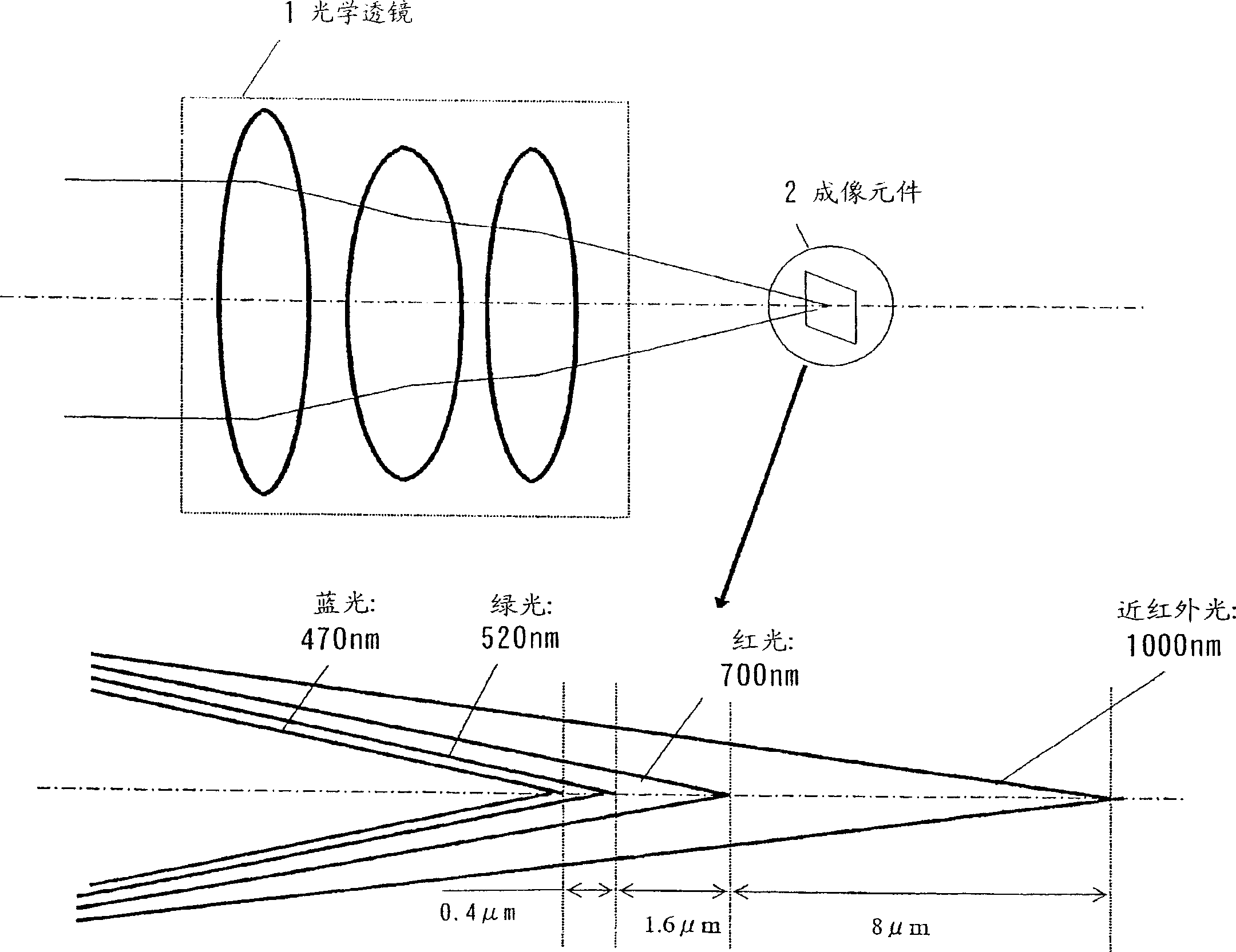
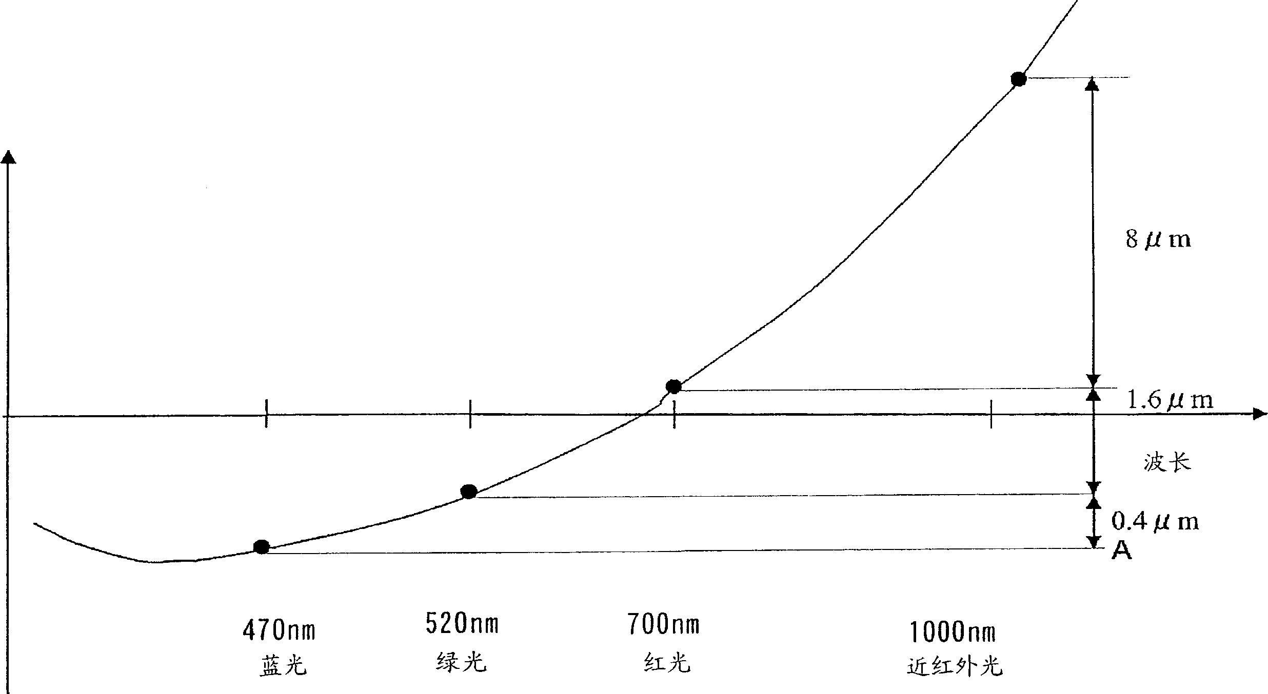
[0041] Such as figure 1 As mentioned above, the visible light and near-infrared light imaging device according to the present invention has an optical lens 1 . The optical lens 1 is an optical system whose focal length varies according to wavelength, and causes three components of visible light and near-infrared light in different wavelength regions to form images at positions different according to their wavelengths. The optical lens 1 gathers light from an external object and forms an image on the imaging element 2 . exist figure 1 The lower part of , the light beams from the optical lens 1 are displayed separately through different wavelengths. As described above, the optical lens 1 forms images at different positions depending on the wavelength. this is in figure 2 A more detailed display in . For example, if the 470nm blue light is in focus reference A, the 520nm green light is 0.4μm longer in focus than reference A. Likewise, red light at 700 nm has a focal lengt...

no. 2 example

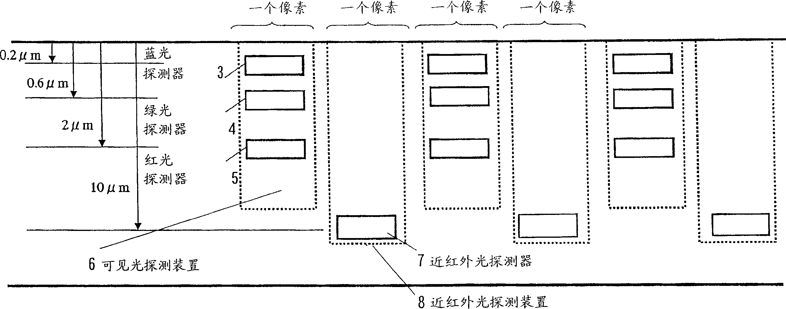
[0060] under, Figure 8 Showing the structure of the imaging element related to the second embodiment, Figure 9 is an equivalent circuit diagram of the imaging element related to the second embodiment. exist Figure 8In the shown imaging element, the visible light detecting portion and the near-infrared light detecting portion are provided in one pixel. The diagram shows a pixel including a detection section to separate and detect three components of visible light and near-infrared light in different wavelength regions, four components in total. In other words, the four current detectors 23, 24, 25, and 26 provided in one pixel detect B, G, and R of visible light and near-infrared light.

[0061] Such as Figure 8 As shown, an n-type doped region 19 of an n-type semiconductor is formed on a p-type semiconductor substrate 9 . Also, a p-type doped region 20 is formed thereon. In addition, an n-type doped region 21 is formed thereon, and a p-type doped region 22 is formed ...


PUM


Abstract

An optical lens 1 makes three components of visible light and near infrared light in different wavelength regions severally form images at different locations according to their wavelengths. An imaging element 2 has a plurality of pixels, which include pixels having a visible light detection section 6 and pixels having a near infrared light detection section 8. The visible light detection section 6 has three detectors 3, 4, and 5 which detect three components of visible light which form images at locations of different depths in the same pixel according to their wavelengths. The near infrared light detection section 8 has a near infrared light detector 7 which detects near infrared light which forms an image at a location of a depth different from the depths at which the three components of visible light form images. Clear color images with good color reproducibility are obtained by the visible light detection section 6, and at the same time clear luminance information or monochrome images are obtained by the near infrared light detection section 8.

Description

technical field [0001] The invention relates to an imaging device and an imaging method, which are used for detecting and receiving three components of visible light and near-infrared light in different wavelength regions, and are used for image formation of visible light and near-infrared light. Background technique [0002] The structure of conventional visible light and near-infrared light imaging devices is as follows: each pixel can detect one of three colors and near-infrared light of different wavelengths in visible light, and such pixels are used in the same imaging element, such as CCD or CMOS imaging element. Hybrid mode settings (for example, Japanese Patent Laid-Open Application No. 2002-142228 figure 2 shown). For example, if Figure 10 As shown, the Mg (magenta) color detector 81, the Ye (yellow) color detector 82, the Cy (cyan) color detector 83, and the near-infrared light detector 84 are mosaically arranged on the imaging element, so that the combination ...

Claims


Application Information

Patent Timeline
Patent Type & Authority Applications(China)
IPC IPC(8): H01L27/146H01L31/10H04N5/335H01L27/14G02B3/00G06T1/00H01L31/101H04N1/028H04N5/369H04N9/04H04N9/07
CPCH04N5/332H04N2209/047H01L27/14645H04N9/045H01L31/101H04N23/11H04N25/131H04N25/17
Inventor 冈田毅石井浩史水泽和史
Owner PANASONIC CORP
Why Eureka
Try Eureka