
Method for operating semiconductor device and semiconductor device

A method of operation, semiconductor technology, applied in the direction of semiconductor devices, electric solid state devices, static memory, etc.

Inactive Publication Date: 2011-12-28
SAMSUNG ELECTRONICS CO LTD
View PDF1 Cites 0 Cited by
  • Summary
  • Abstract
  • Description
  • Claims
  • Application Information

AI Technical Summary

Problems solved by technology

[0004] This leakage current problem is significant for CMOS inverter chains included in integrated semiconductor devices

Method used

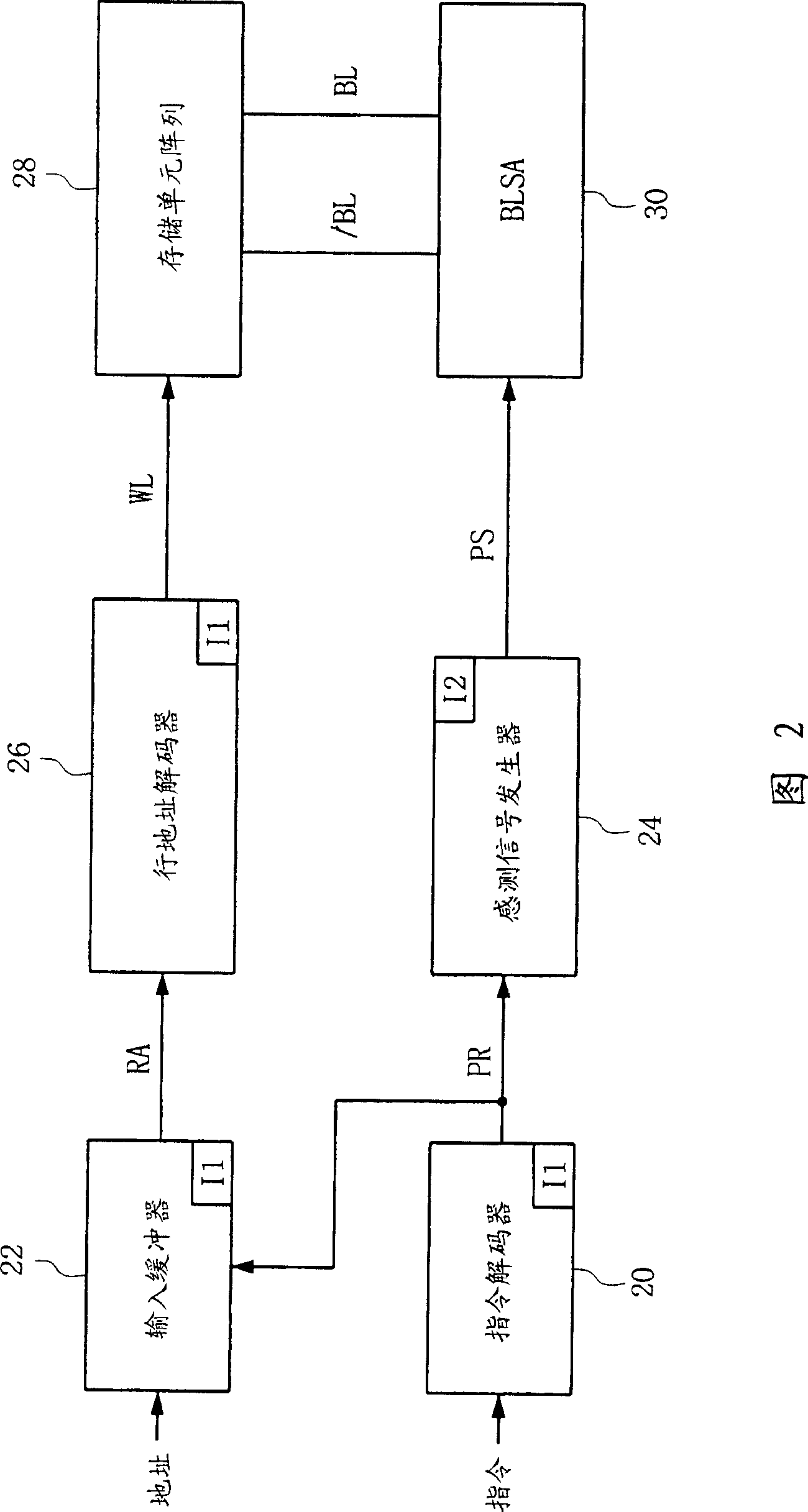
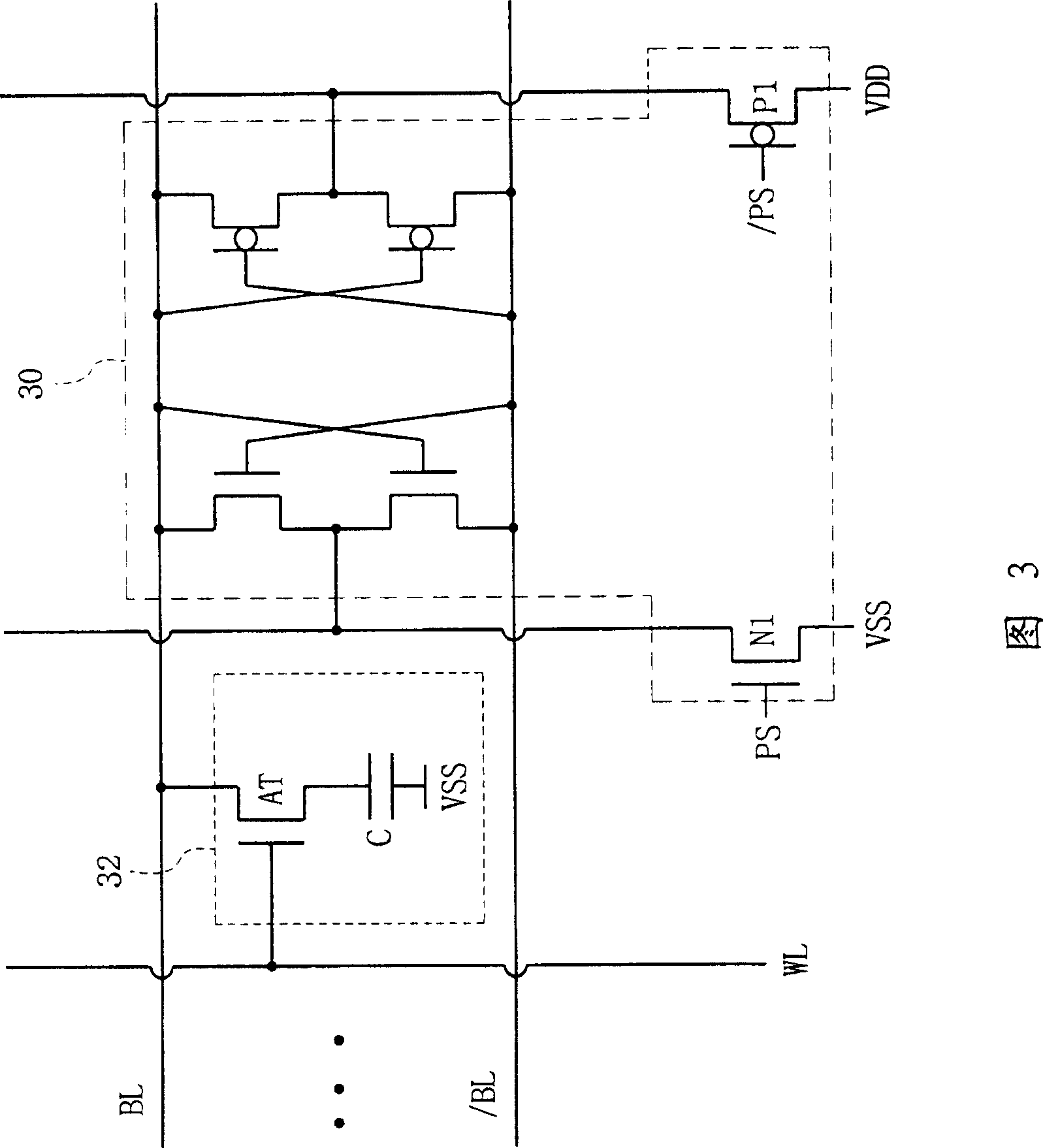

Image

  • Method for operating semiconductor device and semiconductor device
  • Method for operating semiconductor device and semiconductor device
  • Method for operating semiconductor device and semiconductor device

Examples


Embodiment Construction

[0018] An inverter chain according to one embodiment of the present invention will be described, followed by an integrated semiconductor device incorporating the inverter chain.

[0019] inverter chain

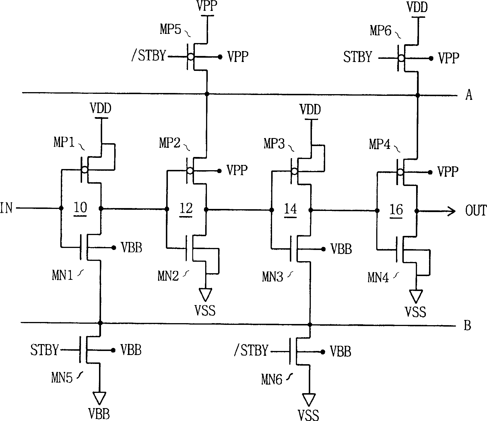
[0020] figure 1 A chain of CMOS inverters according to one embodiment of the invention is shown. As shown, the first-fourth CMOS inverters 10, 12, 14 and 16 are connected in series between the first inverter 10 receiving the input IN and the fourth inverter 16 generating the output OUT. Each of the first-fourth inverters 10, 12, 14 and 16 includes a PMOS transistor connected in series with an NMOS transistor.

[0021] In particular, the first inverter 10 comprises a first PMOS transistor MP1 connected in series with a first NMOS transistor MN1 between a first high potential or voltage VDD (eg 3 volts) and a low potential or voltage line B. As described in detail below, the low potential line B can carry a first low potential VSS (such as ground) or a second low potential VB...


PUM


Abstract

In one exemplary embodiment, the fast circuit path includes a chain of inverters controllably operated in a slow, low subthreshold leakage current mode or a fast, high subthreshold leakage current mode depending on the operating mode of the semiconductor device. The non-fast circuit path includes a chain of inverters operating in a reduced subthreshold leakage current mode independent of the operating mode of the semiconductor device.

Description

[0001] This application claims the benefit of Korean Patent Application No. 2004-58589 filed on July 27, 2004 and Korean Patent Application No. 2004-69786 filed on September 2, 2004, the contents of which are incorporated herein by reference. technical field [0002] The present application relates to methods of operating semiconductor devices and semiconductor devices, and more particularly, to integrated semiconductor devices and methods of operating that prevent sub-threshold leakage currents in a smarter manner. Background technique [0003] In typical integrated semiconductor devices such as DRAM and SRAM, it is desirable to increase the degree of integration while reducing the supply voltage. To accomplish this, the threshold voltage (eg, gate-source voltage) that turns on a large number of MOS transistors included in the integrated circuit device has been reduced. However, the reduction of the threshold voltage of the MOS transistor corresponding to the power supply v...

Claims


Application Information

Patent Timeline
Patent Type & Authority Patents(China)
IPC IPC(8): G11C11/407G11C11/417G11C7/00G11C8/00H01L27/105
CPCG05F1/465
Inventor 崔硕奎金南钟裵壹万崔钟贤
Owner SAMSUNG ELECTRONICS CO LTD
Learn More