Print circuit board with improved heat rejection structure and electronic device

A technology of printed circuit board and heat dissipation structure, which is applied in the direction of printed circuit parts, printed circuits and circuits connected with non-printed electrical components, and can solve the problems of inability to provide heat dissipation effect, inability to dissipate heat, high heat dissipation rate, etc.

Active Publication Date: 2006-02-08
VIA TECH INC
View PDF0 Cites 5 Cited by
  • Summary
  • Abstract
  • Description
  • Claims
  • Application Information

AI Technical Summary

Problems solved by technology

[0005] However, for high-power chips that generate high heat, the above-mentioned passive cooling cannot provide optimal heat dissipation effect and high heat dissipation rate.
That is to say, the heat generated by the chip is conducted to the printed circuit board through the thermal paste and the metal layer and cannot be dissipated effectively and in a timely manner.

Method used


Image

  • Print circuit board with improved heat rejection structure and electronic device
  • Print circuit board with improved heat rejection structure and electronic device
  • Print circuit board with improved heat rejection structure and electronic device

Examples


Embodiment Construction

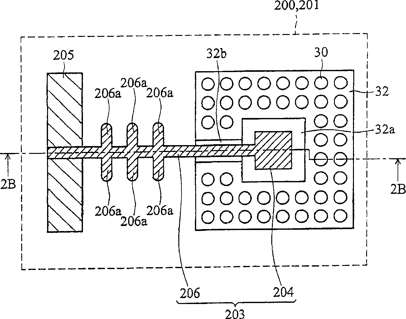
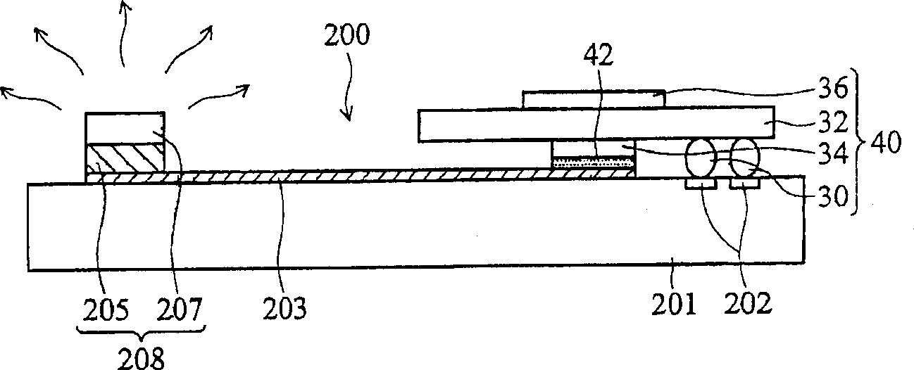
[0030] The following fit Figure 2A and 2B An electronic device with an improved heat dissipation structure is described according to an embodiment of the present invention, wherein Figure 2A A schematic bottom plan view of an electronic device with an improved heat dissipation structure according to an embodiment of the present invention is drawn, and Figure 2B draw the edge Figure 2A Schematic cross-sectional view of line 2B-2B. The electronic device includes: a multi-package module 40 with improved heat dissipation structure, a circuit board 200 and a heat sink 203 .

[0031] Please refer to Figure 3A and 3B ,in Figure 3A A schematic bottom plan view of a multi-package module 40 with an improved heat dissipation structure according to an embodiment of the present invention is shown, and Figure 3B draw the edge Figure 3A Schematic cross-sectional view of line 3B-3B. The multi-package module 40 includes a package substrate 32 . The lower surface of the packag...


PUM


Abstract

This invention discloses a printed circuit board to improve dissipating heat structure, suitable for a packing base plate of multiply packing blocks, which comprises a base plate and a dissipating heat, wherein, dissipating sheets are located on the base plate with a first part located under the pack base plate of multi-pack block, and a second part next to the first part and bearing no less than a fin. The invention also discloses a electron device to better dissipating structure.

Description

technical field [0001] The present invention relates to an electronic device, in particular to an electronic device with an improved heat dissipation structure and a multi-package module (MPM). Background technique [0002] Portable electronic products, such as cell phones, mobile computing and other consumer products need to exhibit high performance and functionality under the constraints of thin thickness, light weight and low cost. Therefore, manufacturers must increase the integration level of semiconductor chips. That is, manufacturers have begun to turn to three-dimensional (3D) packaging, and multiple chips are stacked in one package by assembly techniques such as wire bonding or flip chip. [0003] Therefore, multi-package module (multi-package module, MPM) has recently attracted more and more attention, which can integrate chips with different functions on a package substrate, such as microprocessors or memory, logic and optical integrated circuits, etc., replacing...

Claims


Application Information

Patent Timeline
Patent Type & Authority Applications(China)
IPC IPC(8): H05K1/18H05K7/20H05K1/02H01L27/00H01L23/36
CPCH01L2224/16225H01L2924/15311
Inventor 林志雄张乃舜
Owner VIA TECH INC
Why Eureka
Try Eureka